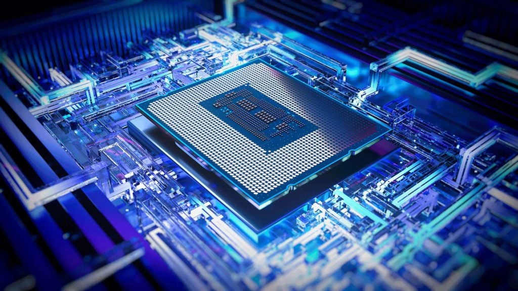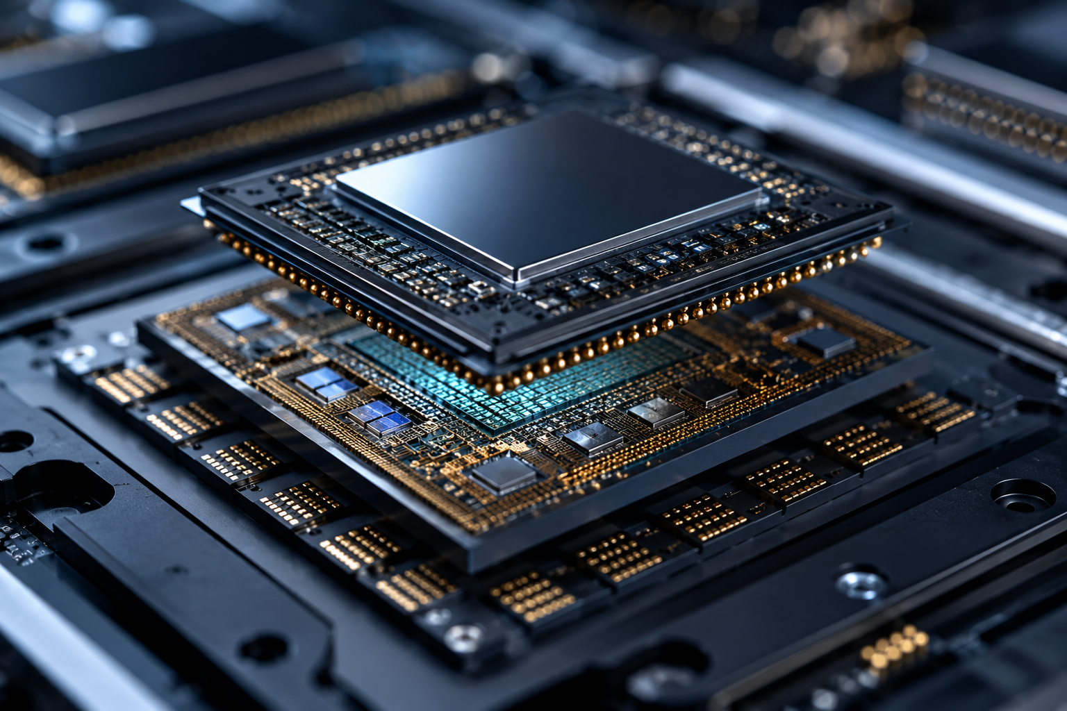
Every time you unlock your smartphone, ask an AI assistant a question, play a realistic video game, or watch a high-definition movie, billions of tiny electronic components spring into action in an instant. Deep inside these devices, computer chips perform unimaginable numbers of calculations every second. But while much attention is given to making transistors smaller and more powerful, another technology has quietly become just as important: advanced chip packaging.
For decades, chip packaging was viewed as little more than a protective shell around a semiconductor chip. Today, that perception has changed completely. Advanced chip packaging has become one of the most important innovations in modern electronics, enabling faster processors, more powerful artificial intelligence systems, improved energy efficiency, and smaller devices than ever before.
As traditional chip scaling becomes increasingly difficult and expensive, engineers are turning to advanced packaging to continue improving computing performance. In many ways, the future of computing now depends not only on how chips are manufactured, but also on how they are packaged together.
Understanding Chip Packaging
Before exploring advanced packaging, it helps to understand what chip packaging actually is.
A semiconductor chip, often called a die, is an incredibly delicate piece of silicon. It contains billions of microscopic transistors and intricate metal wiring. By itself, the silicon die cannot simply be placed inside a smartphone or computer. It needs electrical connections to communicate with the outside world, mechanical support to prevent damage, and protection from moisture, dust, vibration, and heat.
Chip packaging provides all of these functions.
The package acts as the bridge between the tiny silicon chip and the much larger electronic circuit board inside a device. It delivers electrical signals, distributes power, removes heat generated during operation, and protects the chip throughout its lifetime.
Without packaging, even the world’s most advanced processor would be too fragile to use.
Why Traditional Packaging Is No Longer Enough
For many years, chip manufacturers improved computer performance mainly by shrinking transistors. Smaller transistors meant more computing power could fit onto a single chip.
This trend, often associated with Moore’s Law, fueled decades of rapid technological progress.
However, shrinking transistors has become increasingly challenging.
Modern transistors are measured in just a few nanometers—only a handful of atoms across. Manufacturing them requires extraordinary precision, extremely expensive equipment, and highly complex fabrication processes.
As transistor scaling slows, simply making one enormous chip is no longer the best solution.
Large chips have several disadvantages.
They are more difficult to manufacture.
Small defects can ruin an entire chip.
Production costs increase significantly.
Power consumption and heat become harder to manage.
Engineers therefore began looking for another way to improve computing performance without relying entirely on transistor miniaturization.
The answer was advanced chip packaging.
What Is Advanced Chip Packaging?
Advanced chip packaging refers to a collection of technologies that connect multiple semiconductor chips together in highly efficient ways, allowing them to function almost as though they were a single integrated processor.
Instead of building one giant chip containing every function, manufacturers divide complex systems into several smaller chips called chiplets or dies.
These chiplets may each perform different tasks.
One chip might contain CPU cores.
Another may include graphics processing.
A third may provide artificial intelligence acceleration.
Others may handle memory, input and output, networking, or security.
Advanced packaging connects these separate chips using extremely short, high-speed electrical pathways.
The result is a system that offers many of the advantages of a single large chip while avoiding many manufacturing challenges.
Rather than simply protecting the silicon, modern packaging has become part of the computing architecture itself.
Why Chiplets Are Changing Processor Design
One of the biggest innovations enabled by advanced packaging is the rise of chiplets.
Instead of designing one massive processor, engineers create several smaller specialized chips.
These individual chiplets are then packaged together with ultra-fast connections.
This modular approach offers several important advantages.
Smaller chips are easier to manufacture.
Production yields improve because tiny defects affect fewer components.
Manufacturers can reuse chiplet designs across multiple products.
Different manufacturing technologies can be combined within one package.
New processors can be developed more quickly.
This flexibility has made chiplets one of the most important trends in semiconductor engineering.
Many modern high-performance processors already rely on chiplet architectures.
The Difference Between Traditional and Advanced Packaging
Traditional packaging usually places a single silicon die inside one protective package.
Communication between multiple chips occurs through relatively long electrical pathways on the printed circuit board.
Advanced packaging dramatically shortens these distances.
Multiple chips may sit side by side inside the same package.
Some may even be stacked vertically.
Signals travel much shorter distances, allowing information to move faster while consuming less energy.
This improved communication has become essential for artificial intelligence, cloud computing, high-performance computing, and advanced graphics.
Two-Dimensional Packaging
One common form of advanced packaging places multiple chips side by side on a shared substrate.
The substrate acts as a miniature circuit board inside the package itself.
These chips communicate much faster than separate chips mounted elsewhere on the motherboard.
Although this approach remains relatively straightforward, it already provides significant performance improvements over conventional packaging.
Many processors today use this method.
Two-and-a-Half-Dimensional Packaging
A major advancement came with what engineers call 2.5D packaging.
In this design, several chips sit next to one another on a special silicon layer known as an interposer.
The interposer contains extremely fine wiring capable of carrying enormous amounts of data between chips.
Because the connections are much shorter and denser than those found on traditional circuit boards, communication speeds increase dramatically.
This technology is especially valuable for connecting processors with high-bandwidth memory.
Many advanced AI accelerators and graphics processors rely on 2.5D packaging.
Three-Dimensional Packaging
An even more sophisticated approach involves stacking chips vertically.
Instead of arranging chips side by side, engineers place them directly on top of each other.
Special microscopic vertical electrical connections called Through-Silicon Vias (TSVs) carry signals between layers.
This arrangement significantly reduces communication distances.
Data moves almost instantly between stacked chips.
Power efficiency improves.
Overall package size becomes smaller.
Three-dimensional packaging allows enormous computing capability to fit inside surprisingly compact devices.
It is increasingly important for smartphones, data centers, and artificial intelligence hardware.
Through-Silicon Vias
Through-Silicon Vias, often abbreviated as TSVs, are one of the defining technologies behind 3D packaging.
A TSV is a tiny vertical electrical pathway drilled directly through a silicon chip.
These microscopic holes are filled with conductive materials such as copper.
Instead of routing signals around a chip, TSVs allow information to travel directly between stacked layers.
This dramatically increases communication speed while reducing electrical resistance and energy consumption.
Although manufacturing TSVs is technically demanding, they have become essential for many advanced semiconductor products.
Hybrid Bonding
One of the newest breakthroughs in advanced packaging is hybrid bonding.
Rather than using tiny solder bumps to connect chips, hybrid bonding joins both metal and insulating surfaces directly at the microscopic level.
This creates extremely dense electrical connections.
Signals travel faster.
Power consumption decreases.
Heat generation is reduced.
The overall package becomes thinner and more compact.
Hybrid bonding is expected to play a central role in future AI processors, memory technologies, and high-performance computing systems.
High-Bandwidth Memory
Modern artificial intelligence systems process enormous amounts of data.
To keep processors supplied with information, memory must deliver data at extraordinary speeds.
Advanced packaging makes this possible through High-Bandwidth Memory, commonly known as HBM.
Instead of placing memory chips separately on the circuit board, HBM stacks multiple memory dies vertically and positions them very close to the processor.
This arrangement provides exceptionally wide communication channels.
The processor receives data much faster than with conventional memory technologies.
Today’s leading AI accelerators rely heavily on HBM enabled by advanced packaging.
How Advanced Packaging Improves Performance
One reason advanced packaging has become so important is that it improves performance in several different ways simultaneously.
Shorter electrical pathways reduce communication delays.
Signals travel more quickly between chips.
Electrical resistance decreases.
Power efficiency improves.
Heat can often be managed more effectively.
Designers gain greater flexibility in organizing complex computing systems.
These improvements allow processors to perform more calculations while consuming less energy.
This balance between performance and efficiency is especially valuable as artificial intelligence workloads continue expanding.
Better Energy Efficiency
Modern electronics are increasingly limited not by computing power but by electricity consumption.
Large data centers consume enormous amounts of energy.
Smartphones must maximize battery life.
Electric vehicles require efficient onboard computers.
Advanced packaging helps reduce energy use because electrical signals travel much shorter distances.
Less electrical energy is lost during communication.
Lower energy consumption also means less heat is generated.
This creates a positive cycle of improved efficiency throughout the entire system.
Managing Heat
Powerful processors generate significant heat.
Excessive temperatures reduce performance, shorten component lifespan, and may even damage electronics.
Advanced packaging includes sophisticated thermal management techniques.
Special materials transfer heat away from the chip.
Metal heat spreaders distribute thermal energy more evenly.
Innovative package designs improve airflow and cooling.
Some advanced systems even incorporate liquid cooling technologies.
Effective heat management has become one of the most important aspects of modern semiconductor engineering.
The Role of Artificial Intelligence
Artificial intelligence has dramatically increased demand for advanced packaging.
Training large language models and running AI applications require extraordinary computing power.
AI accelerators often combine multiple processing chiplets with stacks of high-bandwidth memory.
Without advanced packaging, these components could not communicate quickly enough.
Packaging therefore enables the massive parallel processing required by today’s AI systems.
As AI models continue growing larger, advanced packaging will become even more essential.
Advanced Packaging in Smartphones
Although advanced packaging is often associated with powerful data centers, smartphones also benefit enormously.
Modern phones contain processors, graphics engines, neural processing units, image processors, security chips, wireless communication systems, and memory—all within an incredibly compact space.
Advanced packaging allows these components to work together efficiently while keeping devices thin, lightweight, and energy efficient.
This contributes to longer battery life, faster performance, improved photography, and enhanced AI capabilities.
Applications Beyond Consumer Electronics
Advanced packaging supports many industries beyond smartphones and computers.
Autonomous vehicles depend on powerful onboard processors capable of analyzing sensor data in real time.
Medical devices increasingly require compact yet highly reliable electronics.
Spacecraft need lightweight systems that can survive harsh environments.
Industrial automation relies on powerful embedded computing.
Telecommunications infrastructure supporting high-speed internet also benefits from advanced semiconductor packages.
As electronics become more capable, advanced packaging becomes increasingly important across nearly every industry.
Manufacturing Advanced Packages
Building advanced semiconductor packages is an extraordinary engineering challenge.
Microscopic chips must be aligned with incredible precision.
Electrical connections may be only a few micrometers wide.
Manufacturing requires specialized equipment capable of placing components with astonishing accuracy.
Engineers carefully inspect each package for defects.
Even tiny misalignments can affect performance.
The manufacturing process often involves dozens of highly controlled steps before the finished package is ready for installation.
Challenges Facing Advanced Packaging
Despite its enormous advantages, advanced packaging also presents several challenges.
Manufacturing complexity continues increasing.
Equipment is expensive.
Thermal management becomes more difficult as more chips occupy smaller spaces.
Testing interconnected chiplets requires sophisticated inspection methods.
Maintaining high manufacturing yields remains challenging.
Researchers around the world continue developing new materials, manufacturing techniques, and package architectures to overcome these obstacles.
The Future of Semiconductor Innovation
For decades, the semiconductor industry relied primarily on transistor scaling to improve performance.
Today, innovation increasingly occurs at the packaging level.
Instead of asking only how to build smaller transistors, engineers now ask how different chips can work together more efficiently.
Future packages may combine processors built using different manufacturing technologies.
Some chiplets may specialize in artificial intelligence.
Others may optimize graphics, communications, security, or memory.
Optical communication technologies may eventually replace some electrical connections within packages.
Researchers are also exploring entirely new packaging materials and architectures that could enable even greater performance.
Advanced packaging is expected to remain one of the fastest-growing areas of semiconductor research throughout the coming decades.
Why Advanced Chip Packaging Matters
Advanced chip packaging represents one of the most important transformations in modern electronics. What was once considered merely a protective enclosure has evolved into a sophisticated technology that directly influences computing performance, energy efficiency, manufacturing cost, and system reliability.
As artificial intelligence, cloud computing, autonomous vehicles, and next-generation consumer electronics demand ever-greater processing power, simply shrinking transistors is no longer enough. Advanced packaging provides a new path forward by bringing multiple specialized chips together into highly integrated systems that communicate with remarkable speed and efficiency.
In many ways, the future of computing will be shaped not only by the silicon inside a chip, but by the ingenious ways engineers connect those chips together. Advanced chip packaging has become the invisible foundation supporting the next generation of technological innovation, ensuring that tomorrow’s electronic devices will be faster, smarter, more efficient, and more capable than ever before.