Modern life runs on tiny pieces of silicon called computer chips. They are hidden inside smartphones, laptops, cars, satellites, medical equipment, gaming consoles, data centers, and even household appliances. Every time you send a message, stream a movie, take a photo, or ask an AI assistant a question, billions of microscopic electronic components are working together inside a chip to make it happen.
Looking at a processor with the naked eye, it seems surprisingly ordinary. It is a small, flat square no larger than a few centimeters across. Yet inside that tiny package lies one of the most sophisticated products humanity has ever created. Manufacturing a modern chip requires extraordinary precision, advanced physics, chemistry, materials science, engineering, and years of research. It is often considered one of the most difficult manufacturing processes ever developed.
Building a skyscraper, launching a spacecraft, or designing a high-speed train are remarkable engineering achievements. Yet manufacturing advanced semiconductor chips may be even more demanding because engineers must build structures thousands of times thinner than a human hair while ensuring that billions of tiny transistors work perfectly together.
So why is chip manufacturing so incredibly complex? The answer lies in the astonishing scale, precision, and scientific challenges involved in turning raw silicon into the brains of modern technology.
What Is a Semiconductor Chip?
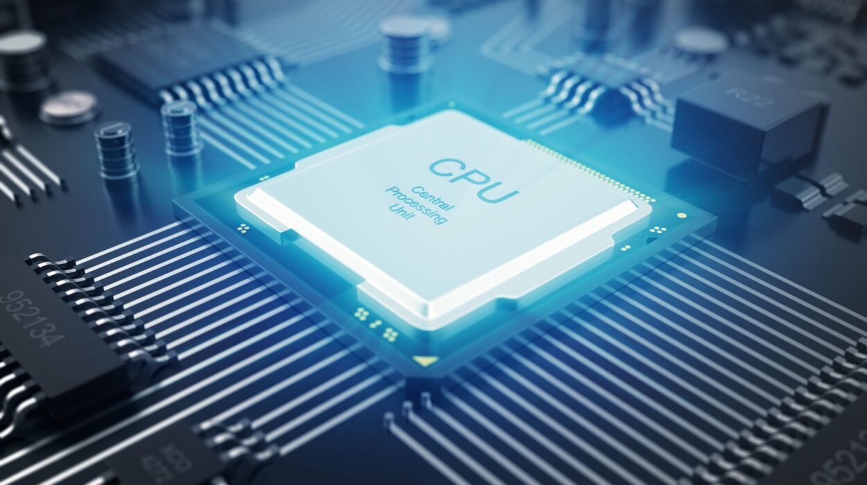
A semiconductor chip, also called an integrated circuit or microchip, is a tiny piece of highly purified silicon that contains millions or even tens of billions of microscopic electronic components. These components include transistors, wires, capacitors, and other structures that process and store information.
The transistor is the fundamental building block of modern electronics. It acts like an extremely fast electronic switch that controls the flow of electricity. Although a single transistor performs a simple task, billions of them working together allow a processor to perform incredibly complex calculations every second.
Today’s most advanced processors contain more than 100 billion transistors. Remarkably, all of these components must fit onto a silicon chip only a few centimeters wide.
Why Smaller Is Better
One reason chip manufacturing has become so challenging is the industry’s constant drive to make transistors smaller.
Smaller transistors allow engineers to place more computing power into the same physical space. This increases processing speed, reduces energy consumption, improves efficiency, and enables thinner, lighter, and more powerful devices.
For decades, semiconductor companies have continuously reduced transistor size. Features inside advanced chips are now measured in nanometers, where one nanometer is one-billionth of a meter.
To appreciate this scale, imagine a human hair. A typical strand of hair is roughly 80,000 to 100,000 nanometers wide. Many structures inside today’s advanced chips are only a few dozen atoms across.
At these dimensions, manufacturing becomes far more difficult because even the smallest imperfection can prevent a chip from working correctly.
Silicon Must Be Almost Perfect
Everything begins with silicon, one of the most abundant elements on Earth. Silicon is found in ordinary sand, but the sand on a beach cannot simply be turned into computer chips.
The silicon used for semiconductor manufacturing must be extraordinarily pure. Even tiny amounts of contamination can affect electrical performance.
Manufacturers first convert raw silicon into an ultra-pure form. The purity reaches astonishing levels, often exceeding 99.9999999 percent. This is far purer than materials used in most other industries.
The purified silicon is melted and slowly grown into a large cylindrical crystal called an ingot. Engineers carefully control temperature, rotation, and growth speed throughout this process because even slight imperfections can ruin the crystal structure.
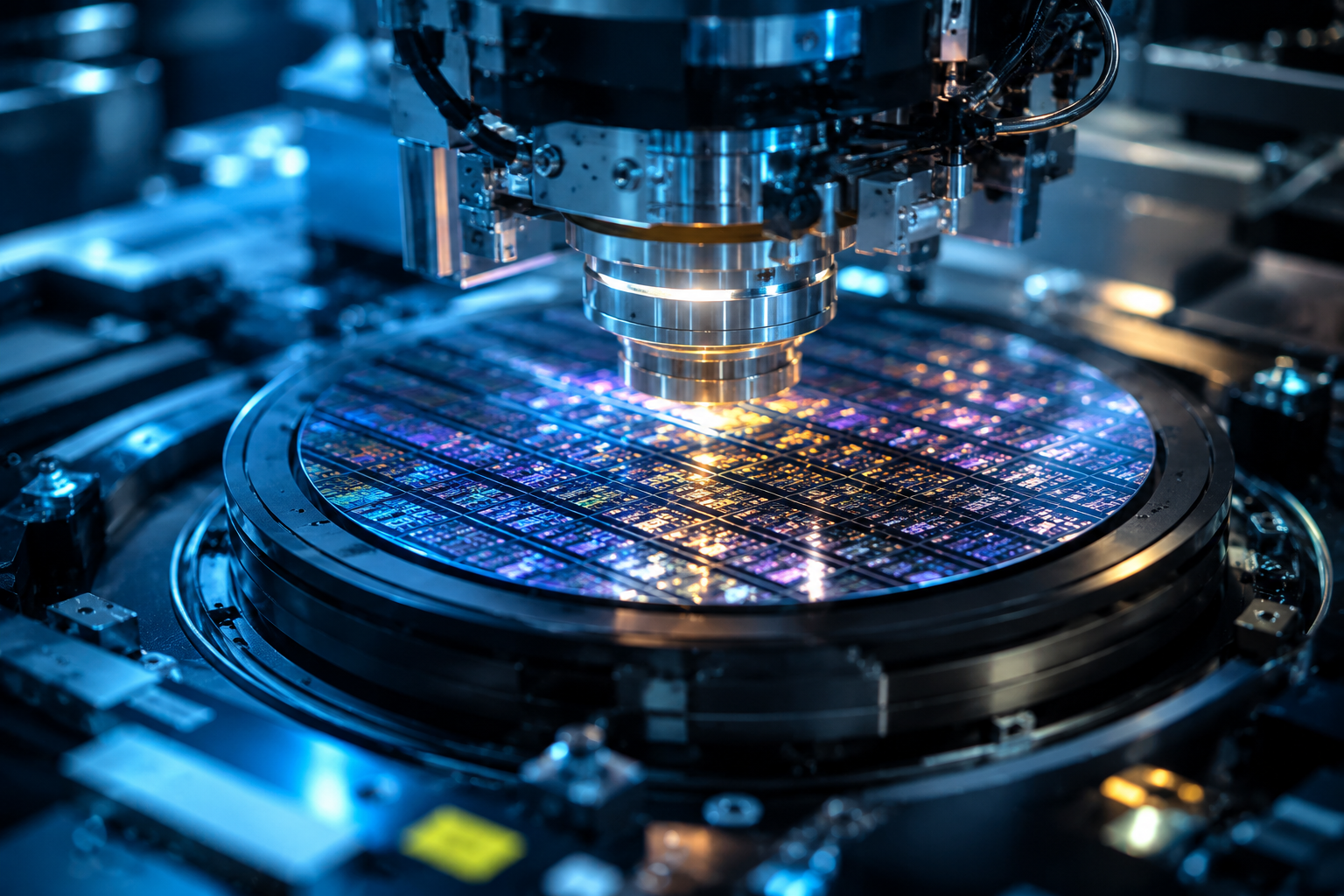
The ingot is then sliced into thin circular discs called wafers. Each wafer becomes the foundation upon which hundreds or even thousands of chips will eventually be manufactured.
The Need for Extraordinary Cleanliness
One of the biggest challenges in chip manufacturing is contamination.
Dust particles that seem invisible to us are enormous compared to transistor features.
Imagine trying to build an entire city where a single grain of sand is larger than a building. That is similar to what engineers face during semiconductor manufacturing.
Because of this, chips are manufactured inside cleanrooms.
These facilities are among the cleanest environments ever created by humans. Powerful filtration systems continuously remove microscopic particles from the air.
Workers wear specialized protective suits that completely cover their bodies. These suits are not primarily designed to protect workers from the chips. Instead, they protect the chips from humans.
A tiny particle of skin, a single hair, or even microscopic droplets released during breathing could damage delicate circuitry.
In the most advanced cleanrooms, the air can be thousands of times cleaner than the air inside a modern hospital operating room.
Creating Patterns Smaller Than Light
One of the most remarkable parts of chip manufacturing is lithography.
Lithography is the process of drawing microscopic circuit patterns onto the silicon wafer.
But engineers cannot simply use ordinary light because visible light has wavelengths that are too large to create extremely tiny features.
Instead, advanced chip factories use extreme ultraviolet light, commonly called EUV light. This light has an extremely short wavelength that allows incredibly fine patterns to be created.
Generating EUV light is itself an engineering marvel.
Tiny droplets of molten tin are fired through a vacuum chamber at astonishing speed. Powerful lasers strike each droplet thousands of times every second, creating an extremely hot plasma that emits EUV radiation.
The light is then reflected—not through ordinary lenses, because EUV is absorbed by most materials—using mirrors polished so perfectly that their surface imperfections are measured in fractions of a nanometer.
If one of these mirrors were enlarged to the size of Earth, its tallest bump would be only a few centimeters high.
Such precision is almost beyond imagination.
Hundreds of Manufacturing Steps
Many people assume a chip is manufactured in only a few stages.
In reality, producing a modern processor often requires well over one thousand individual process steps.
The wafer repeatedly moves through cycles of coating, exposure, chemical treatment, heating, etching, cleaning, measurement, inspection, and deposition.
Each layer adds new microscopic structures.
After one layer is completed, engineers repeat similar processes dozens or even hundreds of times.
Every step must align almost perfectly with the previous ones.
If one layer shifts by only a tiny amount, the entire chip may fail.
Building Multiple Layers
Modern chips are not flat.
Instead, they contain many interconnected layers stacked vertically.
Microscopic metal wires connect billions of transistors together.
Some advanced processors contain more than fifteen layers of metal wiring.
Creating these layers requires remarkable accuracy because each wire must connect exactly where intended.
An error too small for the human eye to detect could disconnect an important circuit or create an unwanted electrical connection.
Working at the Atomic Scale
As transistors become smaller, engineers approach the limits imposed by nature itself.
Atoms are no longer insignificant.
Individual atomic arrangements can influence how a transistor behaves.
At these dimensions, quantum mechanical effects become increasingly important.
Electrons may tunnel through barriers that would normally block them.
Electrical leakage becomes harder to control.
Heat becomes more difficult to remove.
Materials behave differently than they do at larger scales.
Engineers must account for these quantum effects during chip design and manufacturing.
This is one reason semiconductor research depends heavily on modern physics.
Dozens of Different Materials
Although chips are commonly called “silicon chips,” they contain far more than silicon alone.
Modern semiconductor manufacturing uses many carefully engineered materials.
These include specialized metals, insulating materials, chemical compounds, and protective coatings.
Each material performs a specific function.
Some conduct electricity.
Others prevent electrical flow.
Some protect delicate structures during manufacturing.
Others improve transistor performance or reduce electrical resistance.
Choosing the right material requires years of scientific research and testing.
Incredible Precision
Perhaps the greatest challenge in chip manufacturing is precision.
Machines must position wafers with astonishing accuracy.
Some manufacturing equipment aligns layers with precision measured in just a few nanometers.
To appreciate this level of control, imagine accurately placing a single coin on top of another from thousands of kilometers away.
Although this comparison is imperfect, it illustrates the extraordinary engineering involved.
Every machine inside a semiconductor factory must maintain this accuracy continuously while processing thousands of wafers.
Tiny Errors Can Become Big Problems
Manufacturing billions of transistors means even a tiny defect can create problems.
One damaged transistor may prevent an entire processor from functioning correctly.
Manufacturers therefore inspect wafers repeatedly throughout production.
Highly sophisticated imaging systems search for defects that are completely invisible to human eyes.
Artificial intelligence increasingly assists engineers by identifying microscopic problems before they become larger manufacturing failures.
Even after manufacturing is complete, every chip undergoes extensive electrical testing.
Only processors that meet strict performance standards are shipped to customers.
Why Semiconductor Factories Cost So Much
Modern semiconductor fabrication plants, often called fabs, are among the most expensive factories ever constructed.
Building an advanced fabrication facility can cost tens of billions of dollars.
Several factors contribute to these enormous costs.
The buildings require extraordinary environmental control.
The manufacturing machines themselves are incredibly sophisticated.
Many individual tools cost millions of dollars each.
Advanced lithography systems alone can cost hundreds of millions of dollars.
In addition, research, software development, quality control, infrastructure, water purification systems, and energy requirements all contribute to the final cost.
Water Is Surprisingly Important
Chip manufacturing consumes enormous quantities of ultra-pure water.
This water is used repeatedly to clean wafers between manufacturing steps.
Ordinary drinking water is nowhere near pure enough.
Instead, manufacturers produce ultra-pure water by removing almost every dissolved particle, mineral, microorganism, and contaminant.
Some large semiconductor factories process millions of liters of water every day.
Many companies also recycle significant amounts of water to reduce environmental impact.
Temperature Control Matters
Temperature plays an essential role throughout semiconductor manufacturing.
Chemical reactions often require extremely precise temperatures.
Even slight temperature variations can affect transistor dimensions or material properties.
Factories therefore maintain carefully controlled environments to ensure consistent manufacturing conditions.
Equipment also generates substantial heat, requiring sophisticated cooling systems to maintain stable operation.
Why Only a Few Companies Can Make the Most Advanced Chips
Manufacturing leading-edge chips demands decades of accumulated expertise.
It requires thousands of highly trained scientists, engineers, technicians, software developers, chemists, physicists, and materials specialists working together.
Companies must also invest billions of dollars in research every year.
Developing advanced manufacturing techniques takes years, sometimes decades.
Because of these enormous technical and financial barriers, only a small number of companies worldwide possess the capability to manufacture the most advanced semiconductor chips.
Global Cooperation Behind Every Chip
Although individual companies manufacture chips, modern semiconductor production is truly global.
The equipment comes from multiple countries.
The manufacturing chemicals may come from others.
Design software is developed elsewhere.
Raw materials are sourced internationally.
Packaging and testing often occur in different regions before finished chips reach customers around the world.
A single processor may represent contributions from hundreds of companies across dozens of countries.
This global collaboration highlights just how specialized semiconductor manufacturing has become.
Artificial Intelligence Is Increasing the Challenge
The rapid growth of artificial intelligence has dramatically increased demand for powerful chips.
Training advanced AI systems requires enormous computing resources.
Engineers must therefore develop processors that are faster, more energy efficient, and capable of handling increasingly complex calculations.
Meeting these demands requires even smaller transistors, improved manufacturing techniques, advanced packaging technologies, and entirely new chip architectures.
As AI continues advancing, semiconductor manufacturing will likely become even more sophisticated.
The Future of Chip Manufacturing
The semiconductor industry is approaching physical limits that once seemed unimaginably distant.
Researchers are exploring new transistor designs, advanced materials, three-dimensional chip architectures, optical interconnects, quantum devices, and entirely new methods of computation.
Instead of relying only on making transistors smaller, future innovations may focus on stacking chips vertically, improving energy efficiency, integrating specialized AI accelerators, and developing new semiconductor materials beyond traditional silicon.
Scientists are also investigating quantum computing, neuromorphic computing inspired by the human brain, and photonic technologies that use light rather than electricity for certain calculations.
While these technologies remain under active development, they demonstrate that semiconductor innovation is far from over.
Why Chip Manufacturing Represents One of Humanity’s Greatest Engineering Achievements
Every advanced semiconductor chip embodies decades of scientific discovery and engineering excellence. From refining ultra-pure silicon and maintaining some of the cleanest environments on Earth to manipulating light, chemistry, and materials at the nanometer scale, chip manufacturing demands precision that borders on the atomic.
What appears to be a simple black square inside a smartphone or laptop is actually the result of thousands of carefully controlled manufacturing steps, billions of microscopic transistors, and the combined expertise of countless scientists and engineers around the world.
As our reliance on artificial intelligence, cloud computing, autonomous vehicles, medical technology, and space exploration continues to grow, semiconductor chips will become even more essential. Their manufacture will remain one of the most complex, demanding, and remarkable technological accomplishments in human history—a powerful reminder that some of the world’s greatest engineering triumphs are hidden in the smallest objects we use every day.