Every time you unlock your smartphone, power on your laptop, drive an electric car, or connect to the internet, you are relying on one of the most extraordinary materials ever engineered by humanity: the silicon wafer.
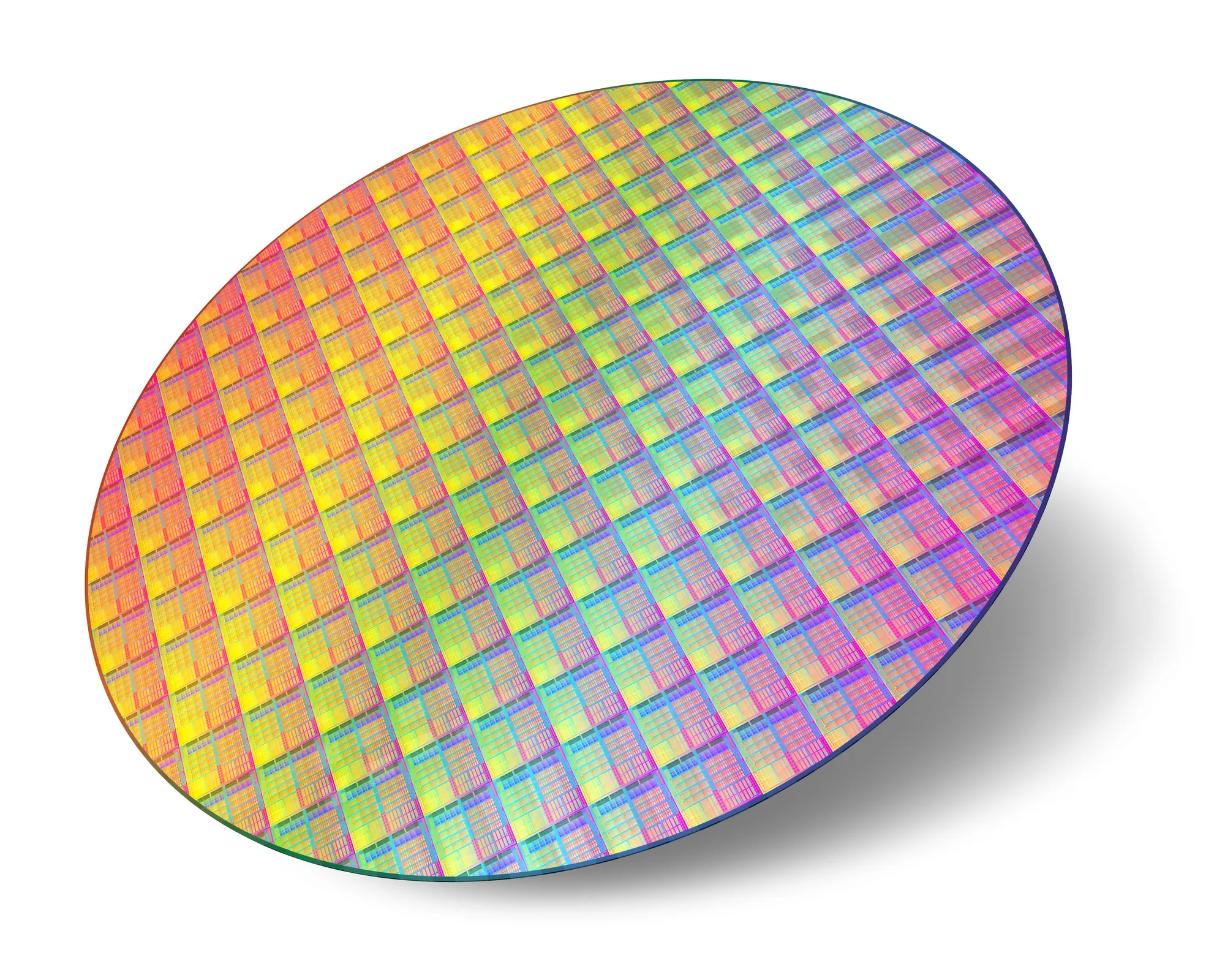
At first glance, a silicon wafer looks surprisingly ordinary. It is simply a thin, shiny, circular disc with a mirror-like surface. Yet beneath that polished appearance lies one of the greatest achievements of modern manufacturing. Each wafer serves as the foundation for hundreds—or even thousands—of computer chips that power nearly every piece of electronic technology in our lives.
What makes this even more fascinating is where the journey begins. The sophisticated processors inside artificial intelligence systems, medical equipment, satellites, and supercomputers all trace their origins to one of Earth’s most common materials: ordinary sand.
Transforming grains of sand into an ultra-pure silicon wafer requires years of scientific innovation, remarkable engineering, and manufacturing precision measured in billionths of a meter. It is a process so demanding that only a handful of companies worldwide can produce the highest-quality wafers used in advanced semiconductor manufacturing.
What Is a Silicon Wafer?
A silicon wafer is a thin, flat slice of highly purified crystalline silicon that serves as the base material for manufacturing semiconductor devices.
Integrated circuits, processors, memory chips, image sensors, power electronics, and countless other electronic components are built layer by layer on top of these wafers.
The wafer itself does not perform calculations or store information. Instead, it acts as an incredibly pure and precisely engineered platform upon which billions of microscopic transistors can be fabricated.
Its surface must be almost perfectly smooth and nearly free from defects. Even an atomic-scale imperfection can affect the performance of the chips eventually manufactured on it.
Why Silicon Is Used
Silicon has become the world’s most important semiconductor material because it possesses a unique combination of properties.
Unlike metals, which conduct electricity extremely well, or insulators, which block electrical flow, silicon falls somewhere in between. This allows engineers to carefully control how electricity moves through it.
By introducing extremely small amounts of other elements into silicon, scientists can create regions that either conduct electricity or resist it. This precise control makes modern transistors possible.
Silicon also forms a high-quality natural oxide, silicon dioxide, when exposed to oxygen under controlled conditions. This oxide plays a critical role in manufacturing integrated circuits.
Another advantage is abundance. Silicon is the second most abundant element in Earth’s crust after oxygen, making it widely available.
Its excellent thermal stability, mechanical strength, and compatibility with advanced manufacturing have made it the dominant material for semiconductor production for decades.
The Journey Begins With Sand
Although silicon is abundant, it does not naturally exist as pure elemental silicon.
Instead, it is commonly found combined with oxygen in minerals such as quartz and silica.
Quartz sand is one of the primary raw materials used in silicon production.
The sand used for semiconductor manufacturing must already be exceptionally clean. High-quality quartz contains very few unwanted impurities compared with ordinary beach sand.
Even so, the quartz is still nowhere near pure enough to manufacture computer chips.
It must undergo multiple stages of purification before it can become semiconductor-grade silicon.
Producing Metallurgical-Grade Silicon
The first major step is converting quartz into elemental silicon.
This is accomplished inside enormous electric arc furnaces operating at temperatures approaching 2,000 degrees Celsius.
Quartz is mixed with carbon-rich materials such as charcoal, coal, or wood chips.
Under intense heat, carbon removes oxygen from the silicon dioxide.
The chemical reaction produces molten silicon and carbon monoxide gas.
After cooling, the resulting material is known as metallurgical-grade silicon.
Although this silicon is around 98 to 99 percent pure, it is still far too contaminated for semiconductor manufacturing.
Tiny amounts of metals such as iron, aluminum, calcium, and many other impurities remain present.
For electronics, even one impurity atom among billions can become a problem.
Achieving Extraordinary Purity
The next stage transforms metallurgical-grade silicon into one of the purest materials ever produced by humans.
First, the silicon reacts with hydrogen chloride gas to produce compounds such as trichlorosilane.
These silicon-containing gases are much easier to purify than solid silicon.
Engineers repeatedly distill the gases, removing unwanted chemical contaminants.
Once purified, the gas enters special reactors where it decomposes at high temperatures.
Pure silicon deposits onto heated silicon rods, gradually forming long, thick cylinders of extremely pure polycrystalline silicon.
This process, known as the Siemens process, can produce silicon with purity exceeding 99.999999999 percent, often referred to as “eleven nines” purity.
At this level, only a few impurity atoms remain among billions of silicon atoms.
Such extraordinary purity is essential because electronic devices depend on precise atomic control.
From Polycrystalline Silicon to a Single Crystal
Although extremely pure, the deposited silicon consists of many small crystals joined together.
Integrated circuits require something much better: one enormous, continuous crystal.
Creating this giant crystal is one of the most remarkable achievements in materials science.
The purified silicon pieces are placed inside a quartz crucible and heated until completely molten at approximately 1,414 degrees Celsius.
A tiny single-crystal silicon seed is then carefully lowered into the liquid.
As the seed slowly rotates and is gradually pulled upward, silicon atoms arrange themselves onto the seed in exactly the same crystal pattern.
This process is called the Czochralski method, named after Polish scientist Jan Czochralski, who invented it in 1916.
Over many hours—or even several days—a massive cylindrical crystal known as an ingot slowly grows.
Some ingots can exceed two meters in length while maintaining nearly perfect crystal alignment throughout.
Why a Single Crystal Matters
The electrical behavior of semiconductors depends heavily on their crystal structure.
If the silicon contained many crystal boundaries, electrons would scatter unpredictably, reducing chip performance and reliability.
A single crystal provides an uninterrupted atomic arrangement across the entire wafer.
This allows electrons to move consistently and predictably.
As transistors continue shrinking toward atomic dimensions, maintaining perfect crystal quality becomes even more important.
Carefully Controlling the Crystal
Growing a silicon crystal is not simply a matter of pulling it upward.
Engineers constantly monitor numerous variables.
The pulling speed must remain carefully controlled.
The crystal rotates at a specific rate.
The crucible often rotates in the opposite direction.
Temperature gradients must remain stable.
Even tiny changes in these conditions can alter crystal quality.
Advanced computer systems continuously adjust the process to ensure the crystal maintains a uniform diameter and minimal defects.
Introducing Precisely Measured Impurities
Although the silicon must be extremely pure, modern electronics require carefully controlled electrical properties.
To achieve this, scientists intentionally add incredibly small amounts of selected elements while the crystal is growing.
Elements such as boron create p-type silicon.
Phosphorus, arsenic, or antimony create n-type silicon.
These additions are called dopants.
The concentration is astonishingly small.
Sometimes only a few impurity atoms exist among millions or even billions of silicon atoms.
Yet these tiny additions determine how the finished semiconductor devices will behave.
Shaping the Crystal
Once the crystal has cooled, it undergoes careful mechanical processing.
The ends are trimmed away because they may contain structural imperfections.
The cylinder is then ground until it reaches an extremely accurate diameter.
Modern semiconductor manufacturing commonly uses wafers measuring 300 millimeters in diameter, although smaller wafers remain common for certain applications.
A small notch or flat edge may also be created to identify the crystal orientation.
This helps manufacturers align the wafer correctly during later fabrication steps.
Slicing the Ingot
The enormous crystal must now be transformed into thin wafers.
This is accomplished using highly specialized wire saws.
A continuously moving wire coated with microscopic diamond particles slices through the crystal with remarkable precision.
Each cut produces a wafer only a fraction of a millimeter thick.
Hundreds of wafers can be obtained from a single crystal ingot.
The slicing process must minimize material loss because producing ultra-pure silicon is extremely expensive.
Making the Surface Perfectly Flat
Freshly cut wafers are not ready for semiconductor manufacturing.
The cutting process leaves microscopic scratches and slight thickness variations.
These imperfections must be removed.
Engineers grind both sides of the wafer until it reaches a highly uniform thickness.
The wafer then undergoes lapping, which further improves flatness.
Chemical etching removes damaged surface layers created during cutting.
Finally, the wafer enters one of the most critical stages: polishing.
Mirror Polishing
Silicon wafers must become extraordinarily smooth.
Manufacturers use chemical mechanical polishing, often abbreviated as CMP.
This process combines gentle mechanical abrasion with carefully controlled chemical reactions.
The result is astonishing.
The finished surface becomes almost perfectly flat.
Surface roughness may measure less than a single nanometer.
To appreciate this precision, imagine shrinking Earth until it becomes the size of a silicon wafer. At that scale, the polished surface would appear smoother than the calmest lake.
This mirror-like finish allows chip manufacturers to create microscopic patterns with incredible accuracy.
Thorough Cleaning
Even after polishing, the wafer cannot be considered clean enough.
Tiny dust particles, organic molecules, metallic contamination, and microscopic residues must all be removed.
Manufacturers perform multiple cleaning steps using specially formulated chemical solutions and ultra-pure water.
The water itself is among the purest ever produced.
Its impurity levels are measured in parts per trillion.
Any contamination remaining on the wafer could damage future semiconductor devices.
Rigorous Inspection
Before wafers leave the manufacturing facility, every one undergoes extensive inspection.
Powerful optical systems search for scratches, particles, pits, cracks, and crystal defects.
Laser-based instruments measure thickness with exceptional accuracy.
Surface flatness is analyzed across the entire wafer.
Crystal orientation is verified.
Electrical properties are carefully checked.
Only wafers meeting extremely demanding specifications continue to semiconductor fabrication plants.
Packaging and Transportation
Once approved, the wafers are packaged inside specially designed protective carriers.
These containers shield the polished surfaces from dust, vibration, moisture, and accidental damage during transportation.
Even microscopic contamination can reduce manufacturing yield.
As a result, great care is taken throughout shipping and storage.
Inside the Cleanroom
Silicon wafer production takes place inside highly controlled cleanrooms.
These environments are vastly cleaner than hospital operating rooms.
Advanced filtration systems continuously remove airborne particles.
Workers wear full-body cleanroom suits that cover nearly every exposed surface.
The clothing is designed not to protect workers from the wafers but to protect the wafers from the workers.
Humans constantly shed skin cells, hair fragments, and microscopic dust.
Any of these particles could interfere with advanced semiconductor manufacturing.
Temperature, humidity, air pressure, and airflow are all carefully controlled.
Why Perfection Is Essential
Modern computer processors contain tens of billions of transistors.
Some of these features measure only a few nanometers across.
At this scale, the smallest crystal defect or contaminant can prevent an entire chip from functioning properly.
Because hundreds or thousands of chips may be manufactured on a single wafer, improving wafer quality significantly increases production yield.
Higher yields reduce manufacturing costs while improving overall reliability.
This is one reason wafer manufacturing demands such extraordinary precision.
Different Wafer Sizes
Over the decades, silicon wafers have steadily grown larger.
Early semiconductor manufacturing used wafers only a few inches across.
Today, the industry standard for advanced logic and memory manufacturing is the 300-millimeter wafer.
Larger wafers allow more chips to be produced during each manufacturing cycle, improving efficiency and lowering costs.
Researchers continue exploring even larger wafer sizes, although the engineering challenges become increasingly complex as diameter increases.
What Happens After the Wafer Is Made?
Producing the silicon wafer is only the beginning.
The polished wafer is delivered to semiconductor fabrication facilities, often called fabs.
There, engineers use advanced lithography, ion implantation, thin-film deposition, plasma etching, and many other sophisticated manufacturing techniques to build integrated circuits.
More than a thousand individual processing steps may occur before the finished chips are complete.
Each transistor, electrical connection, insulating layer, and protective coating is added with astonishing precision.
Eventually, the completed wafer contains hundreds or even thousands of individual chips.
The wafer is then cut into separate pieces, each becoming an individual semiconductor device.
These chips ultimately find their way into smartphones, computers, automobiles, medical equipment, satellites, industrial machinery, artificial intelligence accelerators, and countless other technologies.
The Science Behind Every Digital Device
Although we often admire the finished products—sleek smartphones, powerful laptops, advanced robots, and intelligent AI systems—the true foundation of modern electronics begins long before the first transistor is created.
It begins with an almost impossibly pure crystal of silicon, carefully grown atom by atom, sliced into perfectly flat discs, polished until smoother than nearly any naturally occurring surface, and inspected with extraordinary precision.
Every silicon wafer represents decades of scientific discovery in chemistry, physics, materials science, engineering, and manufacturing. It transforms one of Earth’s most abundant materials into the platform upon which modern civilization is built.
From a humble grain of quartz to the heart of the world’s most advanced microchips, the creation of a silicon wafer is a remarkable journey. It demonstrates how human curiosity, scientific understanding, and engineering excellence can transform ordinary natural materials into the technological foundation of the digital age.