Every time you unlock your smartphone, ask an AI assistant a question, play a high-end video game, edit a 4K video, or watch a movie online, billions of microscopic transistors inside a computer chip begin working almost instantly. These tiny electronic switches perform unimaginable numbers of calculations every second, making modern technology possible.
But have you ever wondered how engineers manufacture these incredibly complex chips?
Creating today’s most advanced semiconductor chips is one of humanity’s greatest engineering achievements. The intricate patterns etched onto a modern processor are so incredibly small that thousands of them could fit across the width of a single human hair. Manufacturing structures at this scale requires a technology unlike anything else ever built.
That technology is called Extreme Ultraviolet Lithography, more commonly known as EUV lithography.
Often described as one of the most complex manufacturing technologies in history, EUV lithography allows chipmakers to create the tiny features needed for the fastest processors, artificial intelligence accelerators, advanced graphics cards, and cutting-edge smartphones. Without EUV, many of the technologies shaping our modern digital world would not exist.
What Is EUV Lithography?
EUV lithography is an advanced manufacturing process used to print extremely tiny circuit patterns onto silicon wafers during semiconductor production.
The word lithography comes from Greek words meaning “writing on stone.” In semiconductor manufacturing, lithography refers to “writing” microscopic electronic circuits onto a silicon wafer using light instead of ink.
Traditional printing presses use visible light and ink to place words on paper.
Chip manufacturers use light to transfer circuit designs onto silicon.
The difference is the astonishing scale.
Instead of letters measured in millimeters, EUV lithography creates patterns measured in nanometers—one billionth of a meter.
A single nanometer is so small that roughly 100,000 nanometers fit across the width of a human hair.
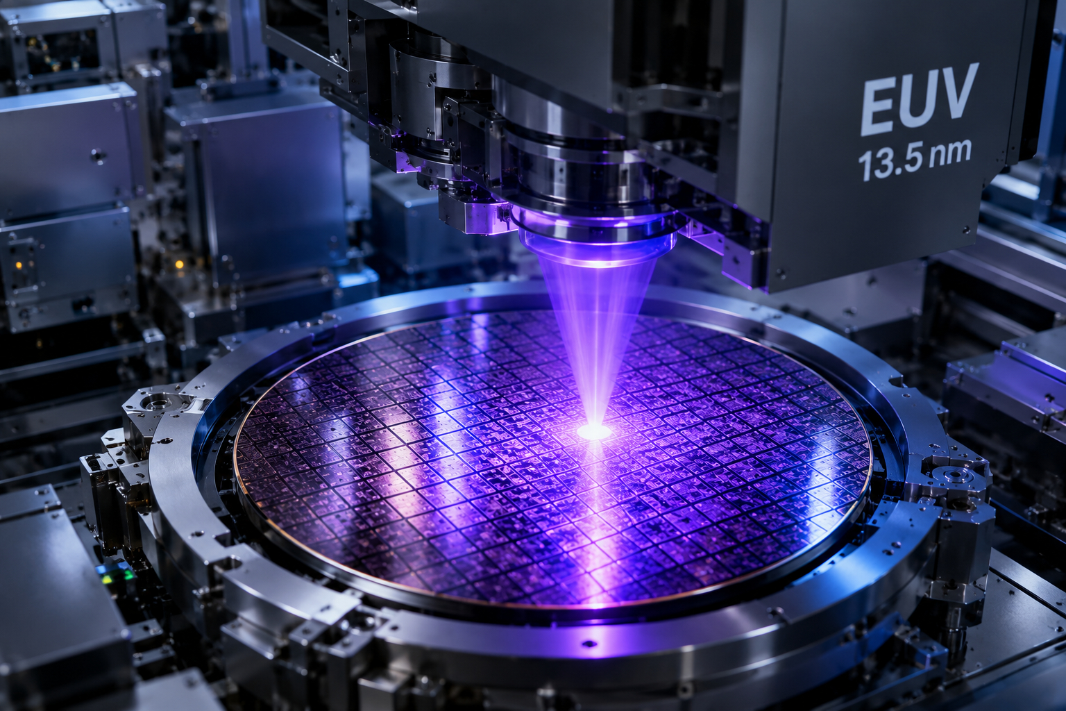
EUV lithography uses an extremely short wavelength of light—only 13.5 nanometers—allowing engineers to print features much smaller than previous technologies could achieve.
Why Modern Chips Need EUV
For decades, the semiconductor industry has continuously reduced transistor sizes.
Smaller transistors offer numerous advantages.
More transistors fit onto each chip.
Computers become faster.
Power consumption decreases.
Heat generation is reduced.
Battery life improves.
Artificial intelligence calculations become more efficient.
However, shrinking transistors eventually creates a fundamental challenge.
The light used for manufacturing chips has a limited ability to produce tiny features.
Imagine drawing extremely detailed artwork with a thick marker.
No matter how carefully you draw, the marker tip is simply too large to create very fine details.
The same principle applies in semiconductor manufacturing.
Older lithography systems used longer wavelengths of ultraviolet light. Eventually those wavelengths became too large to accurately print the smallest transistor features required by modern processors.
EUV solved this problem by using dramatically shorter wavelengths, allowing much finer patterns to be produced.
Understanding Wavelength
To appreciate EUV lithography, it helps to understand wavelength.
Light behaves as an electromagnetic wave.
Each wave has a wavelength—the distance between one peak and the next.
Visible light has wavelengths ranging from roughly 400 to 700 nanometers.
Ultraviolet light has even shorter wavelengths.
Extreme ultraviolet light is shorter still.
The shorter the wavelength, the smaller the details it can produce during lithography.
This relationship is one of the fundamental principles behind modern chip manufacturing.
Using 13.5-nanometer light dramatically increases the resolution available for printing microscopic circuits.
How Lithography Works
At its heart, lithography is surprisingly similar to photography.
Imagine shining light through a stencil onto a surface coated with light-sensitive material.
The illuminated areas undergo chemical changes while protected areas remain unchanged.
Engineers can then remove selected regions to create intricate patterns.
Chip manufacturing follows the same basic concept, although with vastly greater precision.
A polished silicon wafer is first coated with a special light-sensitive chemical called a photoresist.
An optical system directs EUV light through a highly precise mask containing the circuit design.
The projected pattern reaches the wafer.
The exposed photoresist changes chemically.
Subsequent processing removes selected portions of the resist.
The remaining pattern serves as a template for etching microscopic structures into the silicon beneath.
This process repeats dozens of times.
Each layer contributes another part of the finished integrated circuit.
Modern processors may require well over one hundred precisely aligned manufacturing steps before completion.
What Is a Silicon Wafer?
A silicon wafer is a thin, perfectly polished circular slice of extremely pure silicon.
It serves as the foundation upon which integrated circuits are built.
Each wafer contains hundreds—or even thousands—of individual chips depending on their size.
During manufacturing, every chip is created simultaneously across the wafer.
Only after all processing steps are complete are the chips separated and packaged.
Because EUV can print finer patterns, manufacturers can fit more transistors onto each chip, increasing computing power without increasing physical size.
Why EUV Uses Mirrors Instead of Lenses
One of the most fascinating aspects of EUV lithography is that ordinary glass lenses cannot be used.
Glass easily transmits visible light.
However, extreme ultraviolet light behaves very differently.
Almost every material absorbs EUV light.
Even materials transparent to visible light become essentially opaque.
As a result, conventional lenses simply do not work.
Instead, EUV systems use an extraordinary series of precision mirrors.
These mirrors are not ordinary household mirrors.
Each consists of dozens of alternating ultra-thin layers of different materials deposited with atomic precision.
Together, these multilayer coatings reflect EUV light much more efficiently than any conventional mirror could.
Even then, each mirror reflects only part of the incoming light.
Because every reflection loses some energy, generating sufficient EUV light is itself an enormous engineering challenge.
Creating EUV Light
Producing extreme ultraviolet light is one of the most remarkable achievements in modern engineering.
Instead of using an ordinary lamp, EUV machines generate light through an incredibly energetic process.
Tiny droplets of molten tin are released into a vacuum chamber.
Each droplet is only a few tens of micrometers across.
Powerful lasers strike these droplets with extraordinary precision.
The laser energy instantly converts the tin into an extremely hot plasma.
This plasma reaches temperatures approaching hundreds of thousands of degrees Celsius.
At these temperatures, the plasma emits extreme ultraviolet light.
Special mirrors collect and direct the EUV radiation toward the optical system that ultimately projects circuit patterns onto the silicon wafer.
The entire process occurs millions of times every second during operation.
Why a Vacuum Is Essential
Air may seem transparent to us, but it completely absorbs extreme ultraviolet light.
Even a short distance through ordinary air would eliminate nearly all EUV radiation.
For this reason, the entire optical path inside an EUV lithography machine operates under an extremely high vacuum.
Without this vacuum environment, the light would never reach the wafer.
Maintaining such a vacuum while simultaneously controlling lasers, mirrors, moving wafers, and high-speed manufacturing is an extraordinary engineering accomplishment.
The Incredible Precision of EUV Machines
Modern EUV systems are among the most precise machines ever built.
Tiny positioning errors measured in mere nanometers could ruin an entire semiconductor wafer.
The wafer stage moves rapidly while maintaining astonishing positional accuracy.
The optical mirrors are polished so perfectly that their surface imperfections are measured in fractions of a nanometer.
If these mirrors were enlarged to the size of Earth, their tallest imperfections would be only a few centimeters high.
Such extraordinary precision is necessary because every transistor must be printed almost perfectly.
Even microscopic errors can affect chip performance or cause complete failure.
Multiple Layers Build a Modern Chip
A semiconductor chip is not printed in a single step.
Instead, it is built layer by layer.
Each layer performs different electrical functions.
Some layers form transistor gates.
Others create insulating materials.
Additional layers connect billions of transistors through intricate networks of microscopic metal wires.
Each new layer must align almost perfectly with every previous layer.
Modern lithography systems achieve alignment accuracy measured in just a few nanometers.
This capability allows billions of transistors to function together reliably.
Why Smaller Transistors Matter
Reducing transistor size has transformed computing for decades.
Smaller transistors switch more quickly.
Signals travel shorter distances.
Power consumption decreases.
Heat production falls.
More computing capability fits into the same physical area.
These improvements allow smartphones to outperform desktop computers from only a few decades ago.
Artificial intelligence systems can process enormous datasets.
Scientific simulations become increasingly realistic.
Medical imaging improves.
Autonomous vehicles gain greater computing capability.
All of these advances depend, in part, on manufacturing technologies like EUV lithography.
The Connection Between EUV and Moore’s Law
For many years, the semiconductor industry followed a trend known as Moore’s Law.
It observed that the number of transistors on integrated circuits tended to double approximately every two years, leading to rapid improvements in computing power.
Although Moore’s Law is not a physical law, it accurately described industry progress for decades.
Maintaining this pace became increasingly difficult as transistor dimensions approached atomic scales.
EUV lithography became one of the key technologies enabling continued transistor scaling into the modern era.
While engineering challenges continue to grow, EUV has significantly extended the industry’s ability to manufacture increasingly powerful chips.
Where EUV Chips Are Used
Many of today’s highest-performance chips depend upon EUV manufacturing.
Advanced smartphone processors use EUV to improve speed while extending battery life.
Artificial intelligence accelerators rely on enormous numbers of transistors to perform deep learning calculations.
Modern graphics processors benefit from higher transistor densities for gaming, scientific visualization, and machine learning.
Data centers use EUV-manufactured processors to power cloud computing and online services.
Supercomputers perform climate modeling, medical research, astrophysical simulations, and complex engineering calculations using chips produced with advanced lithography techniques.
Even future autonomous robots and intelligent devices will increasingly depend upon semiconductors manufactured using EUV.
Engineering Challenges
Although EUV is revolutionary, it remains extremely difficult.
Generating enough EUV light requires tremendous laser power.
Maintaining mirror cleanliness is essential because even tiny contaminants reduce performance.
Thermal expansion must be carefully controlled.
Mechanical vibrations must be minimized.
Optical alignment requires extraordinary precision.
Manufacturing yields must remain high despite the complexity of the process.
Every component inside an EUV system represents years of engineering research.
The successful integration of these technologies into reliable manufacturing equipment is considered one of the greatest achievements in industrial engineering.
Beyond EUV: High-NA EUV
As transistors continue shrinking, engineers are already developing the next generation of lithography.
One important advancement is High Numerical Aperture EUV, often called High-NA EUV.
Numerical aperture describes an optical system’s ability to capture and focus light.
Higher numerical aperture enables even finer image resolution.
High-NA EUV uses redesigned optics capable of printing even smaller transistor features with greater accuracy.
This technology is expected to support future semiconductor generations requiring even greater transistor densities.
Although extremely challenging to develop, High-NA EUV represents the next step in advanced chip manufacturing.
How EUV Supports Artificial Intelligence
Artificial intelligence systems require enormous computational power.
Training large AI models involves trillions of mathematical operations.
Running these models efficiently depends upon processors containing billions of transistors.
By enabling denser, faster, and more energy-efficient chips, EUV lithography indirectly supports the rapid growth of AI technologies.
From language models and image recognition to robotics and scientific research, increasingly capable AI hardware depends on advances in semiconductor manufacturing.
The Global Importance of EUV
Modern economies rely heavily on advanced semiconductors.
They power communication networks, transportation systems, healthcare equipment, scientific instruments, financial infrastructure, industrial automation, and national security technologies.
Because EUV is essential for manufacturing the world’s most advanced chips, it has become strategically important for many countries.
Governments, research institutions, and semiconductor companies continue investing heavily in lithography research to support future technological progress.
The development of EUV represents decades of international collaboration involving physicists, chemists, materials scientists, optical engineers, software developers, mechanical engineers, and manufacturing specialists.
The Future of Semiconductor Manufacturing
The future of chip manufacturing will continue pushing the boundaries of physics and engineering.
Researchers are exploring improved photoresists, brighter EUV light sources, more efficient mirrors, advanced computational lithography, new transistor architectures, and entirely new semiconductor materials.
As device dimensions approach only a few atoms across, engineers face challenges that blend quantum mechanics, materials science, optics, plasma physics, and nanotechnology.
Future breakthroughs may involve technologies that today seem as revolutionary as EUV once did.
A Triumph of Human Ingenuity
EUV lithography is far more than a manufacturing technique. It is the culmination of decades of scientific discovery and engineering innovation across multiple disciplines. By harnessing light with a wavelength of just 13.5 nanometers, controlling mirrors polished with atomic-level precision, generating plasma hotter than the surface of the Sun, and aligning microscopic patterns with astonishing accuracy, engineers have made it possible to manufacture some of the most advanced devices ever created.
Every new generation of smartphones, powerful computers, AI processors, and cutting-edge electronics reflects the remarkable capabilities of EUV lithography. As humanity continues demanding faster computing, more intelligent machines, and increasingly sophisticated technologies, EUV will remain one of the foundational innovations enabling the digital future.