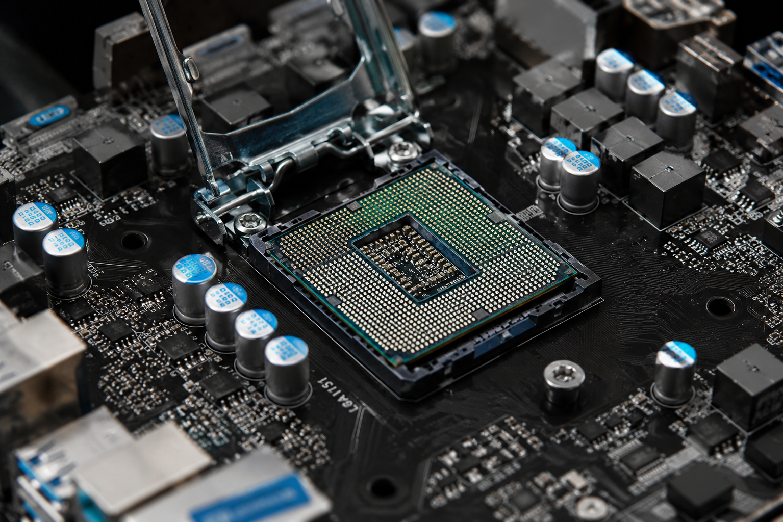
Every time you unlock your smartphone, send a message across the globe, watch a movie on a smart TV, drive a modern car, or ask an AI assistant a question, countless semiconductors spring into action. These tiny pieces of engineered material perform billions—and often trillions—of calculations every second, quietly making modern life possible.
Although they are smaller than a fingernail, semiconductors have transformed human civilization more profoundly than perhaps any other technology of the past century. They are the foundation of computers, smartphones, medical equipment, satellites, electric vehicles, renewable energy systems, artificial intelligence, and even the spacecraft exploring distant planets.
Yet despite their importance, many people have only a vague idea of what a semiconductor actually is or how it works.
The remarkable story of semiconductors begins not in a factory, but deep inside the atoms of one of Earth’s most abundant elements: silicon.
What Is a Semiconductor?
A semiconductor is a material whose ability to conduct electricity lies between that of a conductor and an insulator. Unlike metals, which allow electric current to flow easily, or materials such as glass and rubber, which strongly resist electrical current, semiconductors can behave as either conductors or insulators depending on the conditions.
This unique ability makes semiconductors incredibly useful. Engineers can precisely control when electricity flows, how much flows, and where it goes. This level of control is what allows computers to perform calculations, smartphones to process images, and memory chips to store information.
The word “semiconductor” literally means “partial conductor.” However, this simple description barely hints at the extraordinary physics that gives these materials their remarkable properties.
Why Silicon Became the World’s Most Important Semiconductor
Although several materials can act as semiconductors, silicon has become the dominant choice for modern electronics.
Silicon is the second most abundant element in Earth’s crust, making it relatively inexpensive and widely available. It is found in sand, quartz, and many common rocks.
Beyond its abundance, silicon possesses nearly ideal electrical characteristics. It remains stable over a wide range of temperatures, can be purified to an extremely high degree, and naturally forms a high-quality insulating layer called silicon dioxide. This oxide layer plays a crucial role in manufacturing modern transistors and integrated circuits.
Because of these advantages, silicon became the foundation of the global semiconductor industry.
Today, billions of silicon chips are manufactured every year.
Understanding Electricity Begins with Atoms
To understand how semiconductors work, it helps to first understand the structure of atoms.
Every atom consists of a dense nucleus surrounded by electrons.
The nucleus contains positively charged protons and electrically neutral neutrons.
The electrons carry negative electric charge and occupy regions around the nucleus called electron shells.
Electricity is simply the movement of electrons through a material.
In metals such as copper, many electrons are free to move. As a result, electric current flows easily.
In insulating materials like rubber, electrons are tightly bound to their atoms and cannot move freely. Electricity therefore struggles to pass through.
Semiconductors occupy an unusual middle ground.
Under normal conditions, relatively few electrons move freely.
However, under carefully controlled conditions, many more electrons can begin moving, allowing the material to conduct electricity.
This ability to switch between conducting and insulating behavior is what makes semiconductors so powerful.
The Importance of the Outer Electrons
Silicon atoms each contain fourteen electrons.
The four electrons in the atom’s outermost shell are especially important.
These outer electrons form strong covalent bonds with neighboring silicon atoms.
In a crystal of pure silicon, every atom shares electrons with four surrounding atoms, creating a highly organized crystal lattice.
Because nearly all the outer electrons participate in these bonds, very few electrons remain free to carry electric current.
Pure silicon therefore behaves almost like an insulator at room temperature.
But nature provides a fascinating solution.
Heat gives some electrons enough energy to escape their chemical bonds.
Once free, these electrons can move through the crystal, allowing a small electrical current to flow.
Even more importantly, engineers have discovered ways to dramatically increase this conductivity.
Energy Bands Explain Everything
One of the most important ideas in semiconductor physics is the concept of energy bands.
According to quantum mechanics, electrons inside solids cannot possess arbitrary amounts of energy.
Instead, they occupy allowed energy ranges called energy bands.
Two bands are especially important.
The valence band contains electrons that remain attached to atoms and participate in chemical bonds.
Above it lies the conduction band.
Electrons reaching the conduction band become free to move throughout the crystal, allowing electrical current to flow.
Separating these bands is the band gap.
In conductors, the valence and conduction bands overlap, so electrons move freely.
In insulators, the gap is extremely large, preventing electrons from crossing.
Semiconductors possess a moderate band gap.
With enough energy from heat, light, or an electric field, electrons can cross this gap and begin conducting electricity.
This carefully balanced band gap is the secret behind semiconductor technology.
Electrons and Holes Work Together
When an electron gains enough energy to leave the valence band and enter the conduction band, something equally important happens.
It leaves behind an empty position where the electron used to be.
Physicists call this empty position a hole.
Although a hole is not a physical particle, it behaves like one.
Because neighboring electrons continually move to fill nearby holes, the hole itself appears to travel through the crystal.
Engineers often describe holes as carrying positive charge because their motion is opposite to the movement of electrons.
Electrical current in semiconductors is therefore carried by both electrons and holes.
This dual-carrier system makes semiconductor behavior fundamentally different from ordinary metals.
Pure Silicon Is Only the Beginning
While pure silicon conducts electricity slightly, it is not conductive enough for most electronic devices.
The real breakthrough comes through a process called doping.
Doping involves adding tiny amounts of carefully chosen impurity atoms into the silicon crystal.
Remarkably, only a few impurity atoms among millions of silicon atoms can dramatically alter the material’s electrical behavior.
These impurities are introduced with astonishing precision during semiconductor manufacturing.
Creating N-Type Semiconductors
Suppose engineers add phosphorus atoms to silicon.
Phosphorus has five outer electrons instead of silicon’s four.
Four electrons participate in chemical bonds with neighboring silicon atoms.
The fifth electron has no bond to occupy.
Because it is only weakly attached to the phosphorus atom, very little energy is needed to free it.
This extra electron becomes available for electrical conduction.
Silicon doped in this way is called an N-type semiconductor.
The “N” stands for negative because electrons become the majority charge carriers.
Creating P-Type Semiconductors
Now imagine adding boron atoms instead.
Boron possesses only three outer electrons.
One chemical bond therefore remains incomplete.
This missing electron creates a hole.
Nearby electrons constantly move to fill the hole, causing the hole itself to appear to move through the crystal.
Silicon doped with boron becomes a P-type semiconductor.
The “P” stands for positive because holes become the majority charge carriers.
What Happens When N-Type and P-Type Meet?
One of the greatest discoveries in electronics occurs when N-type and P-type semiconductors are joined together.
The boundary between them forms what scientists call a PN junction.
Initially, electrons from the N-type side naturally diffuse toward the P-type side.
At the same time, holes diffuse in the opposite direction.
As electrons and holes meet, they recombine.
This process leaves behind electrically charged atoms that cannot move.
A special region forms near the boundary where almost no free charge carriers remain.
This region is called the depletion region.
The depletion region creates an internal electric field that strongly influences how electricity flows.
This simple structure forms the basis of nearly every modern electronic device.
The PN Junction Acts Like an Electrical Gate
A PN junction behaves differently depending on the direction of the applied voltage.
When the positive terminal connects to the P-type side and the negative terminal connects to the N-type side, the depletion region becomes narrower.
Electrons and holes can cross the junction more easily.
Current flows.
This condition is called forward bias.
If the voltage is reversed, the depletion region widens.
Charge carriers struggle to cross the junction.
Current nearly stops.
This condition is called reverse bias.
The ability to allow current in one direction while blocking it in the other makes the PN junction the foundation of diodes.
How Diodes Work
A diode is one of the simplest semiconductor devices.
Its primary purpose is controlling the direction of electric current.
Diodes convert alternating current into direct current inside power supplies.
They protect circuits from reverse voltage.
They detect radio signals.
They regulate voltage.
Light-emitting diodes, commonly known as LEDs, produce light when electrons recombine with holes.
Different semiconductor materials produce different colors of light.
Modern LED lighting is highly energy-efficient because it converts much more electrical energy into visible light than traditional incandescent bulbs.
The Transistor Changed the World
The transistor is often considered the most important invention of the twentieth century.
Invented in 1947, it replaced bulky vacuum tubes and made modern electronics possible.
A transistor acts as an electronic switch or amplifier.
Tiny electrical signals control much larger currents.
This simple capability allows transistors to perform logical operations inside computers.
Modern processors contain billions of microscopic transistors working together.
Each transistor rapidly switches between ON and OFF states.
These two states represent the binary digits 1 and 0.
Every calculation performed by a computer ultimately results from enormous numbers of transistors switching billions of times every second.
How a Transistor Works
One of the most common transistors today is the MOSFET, or Metal-Oxide-Semiconductor Field-Effect Transistor.
Rather than physically moving parts, a MOSFET controls electricity using electric fields.
Applying voltage to a component called the gate changes the electrical properties of a tiny channel beneath it.
When sufficient voltage is applied, the channel becomes conductive.
Electrons flow.
Removing the voltage causes the channel to become insulating again.
Current stops.
This incredibly fast electronic switching forms the foundation of digital computing.
Binary Language Inside Computers
Computers do not think using words or numbers the way humans do.
Instead, they process binary information.
Binary uses only two values: 0 and 1.
Each transistor represents one of these states.
Billions of transistors combine to perform addition, multiplication, comparisons, memory storage, image processing, artificial intelligence, and countless other operations.
Although each transistor performs an extremely simple task, billions working together create astonishing computational power.
Integrated Circuits Put Everything Together
Early electronic devices contained individual transistors connected by wires.
As technology advanced, engineers learned to manufacture thousands, then millions, and eventually billions of transistors on a single silicon chip.
These complete electronic systems are called integrated circuits.
Integrated circuits contain not only transistors but also resistors, capacitors, wiring layers, and many other components.
Entire processors, graphics chips, memory devices, and AI accelerators now fit onto chips smaller than a postage stamp.
Why Chips Keep Becoming Smaller
For decades, semiconductor manufacturers have continually reduced transistor size.
Smaller transistors require less power.
They switch faster.
More transistors fit onto each chip.
Computers become faster while consuming less electricity.
Modern transistors are measured in nanometers.
A nanometer equals one billionth of a meter.
At these tiny dimensions, engineers must account for quantum mechanical effects that barely mattered in earlier generations of electronics.
Manufacturing such devices represents one of humanity’s greatest engineering achievements.
How Semiconductor Manufacturing Works
Building semiconductor chips requires extraordinary precision.
The process begins with highly purified silicon.
This silicon is grown into large, nearly perfect cylindrical crystals.
Thin circular slices called wafers are cut from these crystals.
Each wafer undergoes hundreds of manufacturing steps inside extremely clean fabrication facilities known as fabs.
Layers of materials are deposited, etched, and patterned using advanced techniques such as photolithography.
Photolithography projects intricate patterns onto the wafer using ultraviolet light.
These patterns define billions of microscopic transistors and electrical connections.
Modern fabrication facilities are among the most technologically advanced manufacturing environments ever created.
Even microscopic dust particles can ruin an entire chip.
Why Clean Rooms Matter
Semiconductor fabrication takes place inside clean rooms that contain far fewer airborne particles than ordinary air.
Workers wear specialized protective suits to prevent contamination.
Air continuously flows through advanced filtration systems.
Temperature, humidity, vibration, and even tiny electrical disturbances are carefully controlled.
This remarkable level of cleanliness ensures that microscopic circuits are manufactured accurately.
Semiconductors Power Artificial Intelligence
Artificial intelligence depends heavily on semiconductor technology.
AI processors perform enormous numbers of mathematical operations simultaneously.
Graphics Processing Units (GPUs), Tensor Processing Units (TPUs), Neural Processing Units (NPUs), and specialized AI accelerators all rely on billions of advanced transistors.
Without semiconductor innovation, modern machine learning, large language models, image recognition, and autonomous vehicles would not exist.
Semiconductors in Everyday Life
Most people interact with semiconductors hundreds of times each day without realizing it.
Smartphones contain processors, memory chips, camera sensors, wireless communication chips, and power management circuits.
Cars use semiconductor chips to control engines, safety systems, navigation, entertainment, braking, and electric motors.
Medical devices rely on semiconductor sensors and processors to diagnose disease and monitor patients.
Televisions, refrigerators, washing machines, Wi-Fi routers, gaming consoles, drones, satellites, digital cameras, smart watches, and even household light bulbs all depend on semiconductor technology.
Modern society functions because tiny silicon chips quietly manage billions of electronic tasks every second.
Beyond Silicon
Although silicon remains dominant, researchers continue developing new semiconductor materials.
Gallium nitride performs exceptionally well in high-power electronics and fast chargers.
Silicon carbide enables efficient electric vehicle power systems.
Gallium arsenide excels in high-frequency communication and satellite technology.
Scientists are also investigating two-dimensional materials such as graphene and transition metal dichalcogenides for future ultra-thin electronic devices.
These materials may enable faster, smaller, and more energy-efficient electronics in the coming decades.
The Future of Semiconductor Technology
Semiconductor technology continues evolving at an extraordinary pace.
Researchers are exploring three-dimensional chip architectures, advanced packaging techniques, quantum computing hardware, optical computing, neuromorphic processors inspired by the human brain, and entirely new transistor designs.
Artificial intelligence is driving demand for increasingly powerful chips, while energy efficiency has become equally important as computing performance.
As devices become smarter and more connected, semiconductors will remain at the center of technological progress.
The Invisible Foundation of the Digital Age
Semiconductors are among humanity’s greatest scientific and engineering achievements. Their remarkable ability to precisely control the flow of electricity has transformed nearly every aspect of modern civilization. From the quantum behavior of electrons inside silicon crystals to the billions of microscopic transistors inside today’s processors, semiconductors demonstrate how deep scientific understanding can reshape the world.
Although they remain hidden inside electronic devices, their impact is impossible to overlook. Every digital photograph, online conversation, satellite navigation system, medical diagnosis, scientific simulation, and artificial intelligence breakthrough depends on these extraordinary materials. As research continues to push the limits of physics and engineering, semiconductors will remain the invisible foundation upon which the future of technology is built.