Every time you unlock your smartphone, stream a movie, ask an AI assistant a question, or drive a modern car, you are relying on one of the greatest manufacturing achievements in human history. Hidden inside these devices are tiny computer chips containing billions of microscopic transistors, all carefully arranged with astonishing precision. But how can engineers create structures so small that thousands of them could fit across the width of a single human hair?
The answer is a remarkable manufacturing process called photolithography.
Photolithography is often described as the heart of semiconductor manufacturing because it allows engineers to transfer incredibly detailed circuit patterns onto silicon wafers. Without it, modern processors, memory chips, graphics cards, AI accelerators, and nearly every advanced electronic device simply could not exist.
Although the process sounds highly technical, its basic idea is surprisingly elegant. It works much like taking a photograph, except instead of capturing an image on photographic film, it projects microscopic circuit patterns onto a silicon wafer with extraordinary accuracy.
What Is Photolithography?
Photolithography is a manufacturing process used to transfer extremely small patterns onto the surface of a semiconductor wafer using light.
The word itself comes from three Greek roots. “Photo” means light, “litho” means stone or writing, and “graphy” means drawing or recording. Together, photolithography essentially means drawing patterns with light.
In semiconductor manufacturing, these patterns become the tiny electrical pathways, transistor gates, contacts, and other structures that make integrated circuits function.
Each layer of a computer chip is created by repeating the photolithography process many times. Modern processors often require dozens or even hundreds of individual patterning steps before the chip is complete.
Why Photolithography Is So Important
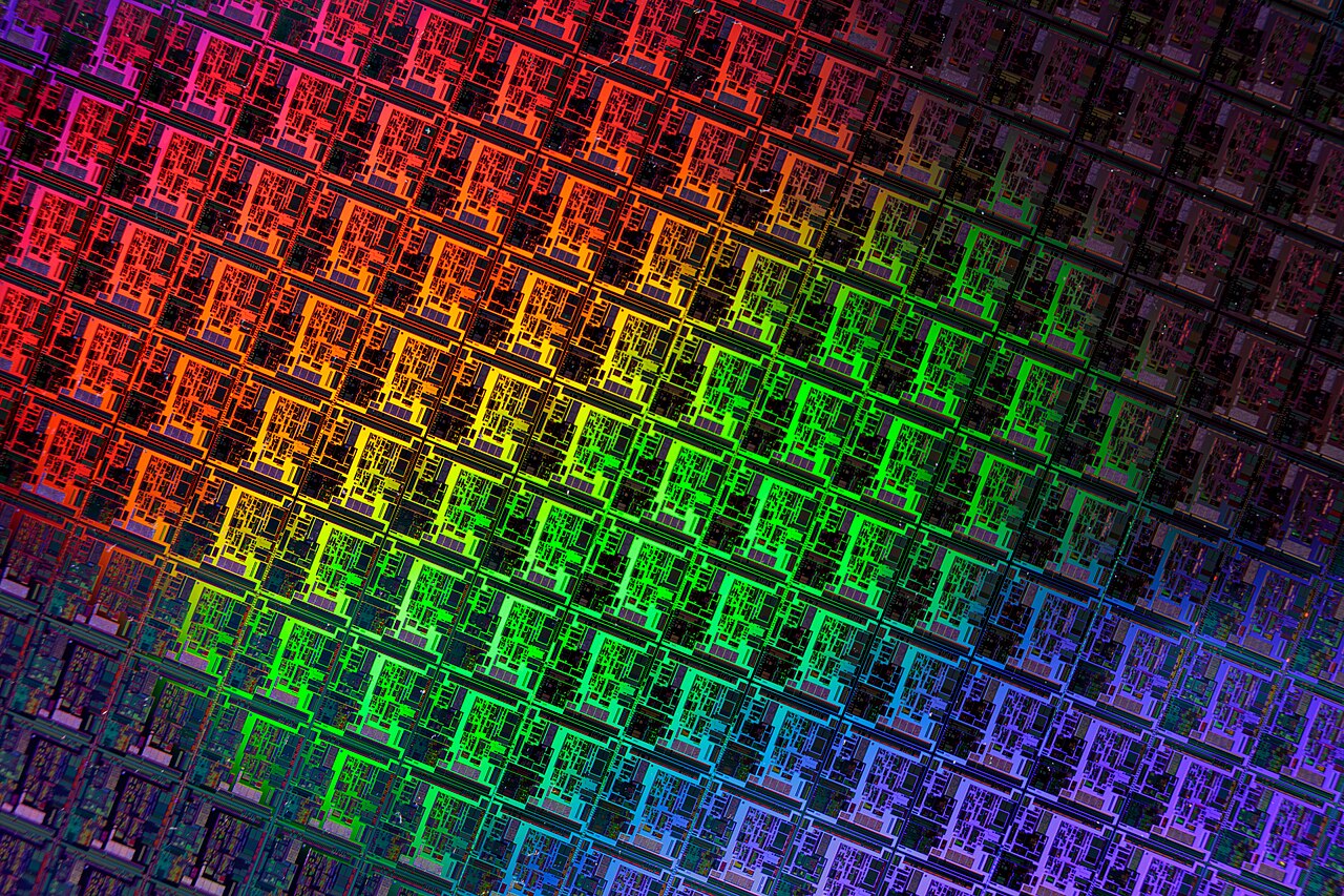
A modern microprocessor may contain tens of billions of transistors.
Every one of these transistors must be placed in exactly the right position.
Even an error measured in just a few nanometers could prevent the chip from working.
Photolithography provides the precision needed to manufacture these incredibly complex designs.
Without it, today’s technologies would be impossible.
Artificial intelligence processors, smartphones, laptops, cloud computing, satellites, medical equipment, gaming consoles, autonomous vehicles, and advanced communication systems all depend on chips produced using photolithography.
The Silicon Wafer: Where Every Chip Begins
Before photolithography begins, manufacturers prepare a highly polished silicon wafer.
A silicon wafer is an extremely thin, circular slice of nearly pure crystalline silicon.
Silicon is chosen because its electrical properties make it an excellent semiconductor. Its conductivity can be carefully controlled by introducing tiny amounts of specific elements, allowing engineers to build transistors and other electronic components.
The surface of the wafer must be extraordinarily clean.
Even a dust particle can be much larger than the tiny features engineers are trying to create. A single speck of dust could ruin an entire chip.
For this reason, semiconductor factories operate inside ultra-clean rooms where the air contains far fewer particles than ordinary indoor environments.
The Role of Light
Light is the essential tool of photolithography.
Instead of physically carving tiny patterns into silicon, engineers use carefully controlled light to transfer circuit designs.
The process resembles using a stencil.
Light passes through a precisely designed pattern and exposes only selected parts of the wafer.
Those exposed regions can then be chemically processed while the unexposed regions remain protected.
By repeating this process layer after layer, engineers gradually build the complete integrated circuit.
Understanding the Photomask
One of the most important components in photolithography is the photomask, often simply called a mask.
A photomask is a flat piece of ultra-pure glass coated with an opaque material, usually chromium.
Tiny transparent openings are created in this coating according to the chip’s circuit design.
These openings determine exactly where light passes through.
Each photomask corresponds to one specific layer of the chip.
Since modern processors contain many layers, manufacturing a single chip requires numerous masks, each representing different structures such as transistor gates, electrical connections, or insulating layers.
Creating these masks requires extraordinary precision because any error would be copied onto every chip manufactured.
What Is Photoresist?
The silicon wafer cannot be exposed directly.
Instead, manufacturers coat it with a special light-sensitive chemical called photoresist.
Photoresist behaves somewhat like photographic film.
When exposed to light, its chemical properties change.
Some photoresists become more soluble after exposure, while others become less soluble, depending on their chemical formulation.
This change allows manufacturers to selectively remove specific regions during later processing.
The photoresist layer is incredibly thin, often only a fraction of a micrometer thick.
Engineers apply it evenly by spinning the wafer at high speed, allowing centrifugal force to spread the liquid into a uniform coating.
Aligning the Pattern
Once the photoresist has been applied, the wafer moves into a lithography machine called a stepper or scanner.
Here, engineers carefully align the photomask with the wafer.
Alignment is one of the most critical parts of the entire manufacturing process.
Modern chips contain many layers stacked on top of one another.
Every new layer must line up almost perfectly with all previous layers.
The acceptable alignment error is often measured in just a few nanometers.
Sophisticated optical systems, lasers, cameras, and computer-controlled positioning mechanisms ensure this remarkable accuracy.
Exposing the Wafer
After alignment, ultraviolet light shines through the photomask.
Only light passing through the transparent regions reaches the photoresist.
Where light strikes the photoresist, chemical changes occur.
The exposed pattern now exists invisibly within the photoresist layer.
This latent image resembles the hidden image formed on traditional photographic film before development.
Although invisible to the naked eye, it precisely defines the microscopic circuit structures.
Developing the Pattern
The wafer is then immersed in or sprayed with a chemical developer.
The developer dissolves selected portions of the photoresist.
Exactly which portions dissolve depends on whether a positive or negative photoresist is being used.
After development, part of the silicon surface becomes exposed while the remaining areas remain protected by photoresist.
The microscopic circuit pattern has now been transferred successfully onto the wafer.
Etching the Silicon
The exposed silicon must now be modified.
This usually happens through a process called etching.
Etching removes material from the exposed regions while leaving the protected regions untouched.
There are two primary types of etching.
Wet etching uses carefully controlled liquid chemicals.
Dry etching uses plasma containing highly energetic ions and reactive gases.
Modern semiconductor manufacturing relies heavily on plasma etching because it provides exceptional precision and can create nearly vertical sidewalls, which are essential for advanced transistor designs.
Removing the Photoresist
After etching is complete, the remaining photoresist has finished its job.
Manufacturers remove it using specialized chemical or plasma cleaning processes.
The wafer is now ready for the next manufacturing step.
This cycle is repeated many times during chip fabrication.
Each repetition adds another tiny piece of the final integrated circuit.
Building a Chip Layer by Layer
A modern processor is not created in a single exposure.
Instead, it is built through dozens or even hundreds of carefully controlled manufacturing steps.
Photolithography repeatedly defines different structures.
Some steps create transistor gates.
Others define electrical contacts.
Additional layers create metal wiring that connects billions of transistors together.
Insulating materials separate different conducting layers.
The final result resembles a three-dimensional microscopic city filled with interconnected structures.
Each completed chip is the product of months of manufacturing involving thousands of precisely controlled operations.
Positive and Negative Photoresists
Photoresists fall into two main categories.
Positive photoresists become soluble where light strikes them.
During development, the exposed regions dissolve away.
Negative photoresists behave in the opposite manner.
Exposure causes chemical reactions that harden the material.
The unexposed regions dissolve during development instead.
Both types have advantages depending on the manufacturing process and desired circuit features.
Why Smaller Features Matter
One of the driving goals of semiconductor manufacturing has been reducing feature size.
Smaller transistors allow more components to fit onto each chip.
This generally improves computing performance while reducing power consumption and manufacturing cost per transistor.
As feature sizes have shrunk from micrometers to nanometers, photolithography has become increasingly sophisticated.
Today’s leading-edge manufacturing creates structures measured in only a few dozen atoms across.
Producing such tiny features pushes the limits of both physics and engineering.
The Challenge of Light Wavelength
One fundamental challenge arises from the nature of light itself.
Light behaves as a wave.
Its wavelength limits how small a pattern can be printed directly.
To create ever-smaller transistor features, semiconductor manufacturers have steadily reduced the wavelength of lithography light.
Early systems used visible light.
Later generations adopted deep ultraviolet light.
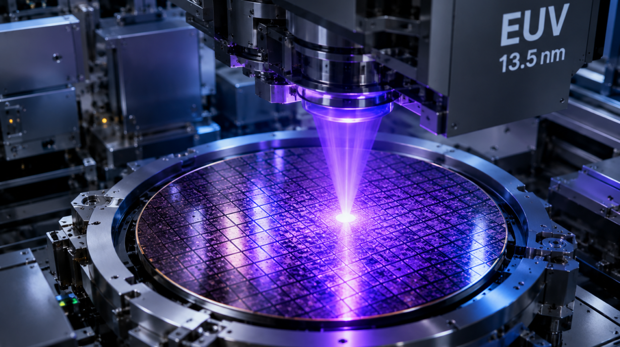
Today, the world’s most advanced semiconductor factories use extreme ultraviolet (EUV) light with a wavelength of approximately 13.5 nanometers.
This extremely short wavelength enables engineers to produce the tiny structures required for modern processors.
What Is Extreme Ultraviolet Lithography?
Extreme ultraviolet lithography, commonly abbreviated EUV, represents one of the greatest engineering achievements in manufacturing.
Producing EUV light is remarkably difficult.
Ordinary light bulbs or lasers cannot generate it efficiently.
Instead, powerful lasers fire tens of thousands of times per second at microscopic droplets of molten tin.
The laser transforms the tin into extremely hot plasma, which emits EUV radiation.
Unlike visible light, EUV cannot travel through ordinary glass because nearly all materials absorb it.
Instead of lenses, EUV systems use extraordinarily smooth mirrors coated with multiple ultra-thin layers that reflect the light.
Each mirror must be polished so perfectly that its surface imperfections are smaller than the size of individual atoms.
The Incredible Precision of Modern Lithography
Modern lithography systems rank among the most complex machines ever built.
Their optical systems contain thousands of precisely manufactured components.
Positioning systems move wafers with nanometer-level accuracy.
Temperature, vibration, humidity, and air quality are continuously controlled.
Even tiny thermal expansion within machine components could reduce manufacturing accuracy.
Engineers therefore maintain extraordinarily stable operating conditions throughout production.
Clean Rooms: Protecting Tiny Circuits
Semiconductor fabrication takes place inside highly controlled clean rooms.
Workers wear specialized protective clothing that covers nearly their entire bodies.
This clothing does not primarily protect workers.
Instead, it protects the wafer from contamination.
A human hair measures roughly 70,000 to 100,000 nanometers in diameter.
Many transistor features are only a few nanometers wide.
A single dust particle could therefore be hundreds of times larger than the structures being manufactured.
Maintaining extreme cleanliness is essential for achieving high manufacturing yields.
Applications of Photolithography
Photolithography is not limited to computer processors.
It is used throughout the semiconductor industry.
Memory chips depend on it.
Graphics processors require it.
Artificial intelligence accelerators use it extensively.
Wireless communication chips, automotive electronics, sensors, power management devices, image sensors inside digital cameras, and countless other integrated circuits all rely on photolithography.
The technique also plays important roles outside semiconductor manufacturing.
It is used in producing microelectromechanical systems, biomedical devices, advanced sensors, microfluidic chips, and certain optical components.
Challenges Facing Modern Photolithography
As transistors continue shrinking, photolithography faces growing technical challenges.
Engineers must manage optical diffraction, material limitations, alignment accuracy, manufacturing cost, and increasing process complexity.
Producing advanced chips now requires extraordinary investments.
A state-of-the-art semiconductor fabrication facility can cost tens of billions of dollars.
The lithography equipment itself ranks among the most expensive manufacturing machines ever constructed.
Despite these challenges, continuous innovation keeps pushing chip technology forward.
The Future of Photolithography
Researchers continue exploring ways to improve photolithography even further.
Future developments may include higher numerical aperture EUV systems capable of printing even finer features.
Scientists are also investigating new photoresist materials, improved optical systems, advanced computational lithography, and entirely new manufacturing techniques.
Artificial intelligence is increasingly being used to optimize lithography processes, improve defect detection, and enhance manufacturing efficiency.
These advances will support future generations of processors designed for artificial intelligence, quantum computing, advanced communications, autonomous vehicles, and scientific research.
How Photolithography Changed the World
Photolithography is one of the hidden technologies that transformed modern civilization.
Most people never see it, yet nearly every electronic device depends on it.
The astonishing computing power found in today’s smartphones, laptops, medical equipment, satellites, and data centers exists because engineers learned how to draw unimaginably small patterns using light.
Each new generation of photolithography has enabled faster processors, larger memories, lower power consumption, and more affordable electronics. It has fueled the rapid growth of computing, the internet, artificial intelligence, and countless scientific breakthroughs.
Although invisible inside every chip, photolithography stands among humanity’s greatest technological achievements. By combining physics, optics, chemistry, materials science, and precision engineering, it allows microscopic designs to become the foundation of the digital world, powering nearly every aspect of modern life and opening the door to technologies that continue to reshape our future.