Every time you unlock your smartphone, start your laptop, stream a movie, or ask an AI assistant a question, billions of tiny electronic switches inside a computer chip begin working almost instantly. These chips perform trillions of calculations every second, quietly powering the digital world we depend on every day.
Yet few people realize that the remarkable devices inside our phones and computers begin as something surprisingly ordinary—sand.
The journey from common sand to one of the most advanced technologies ever created is among the greatest achievements in modern science and engineering. It combines chemistry, physics, materials science, optics, nanotechnology, robotics, and extreme precision manufacturing. Every step must be nearly perfect because even a microscopic speck of dust can ruin a chip worth thousands of dollars.
Understanding how computer chips are made reveals not only the incredible complexity of modern technology but also the extraordinary level of human ingenuity required to build the digital age.
What Is a Computer Chip?
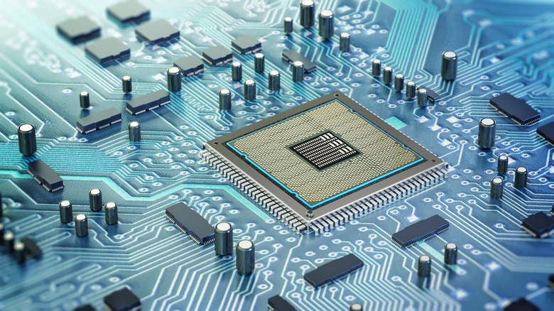
A computer chip, also called an integrated circuit or microchip, is a small piece of semiconductor material that contains millions, billions, or even hundreds of billions of tiny electronic components.
These components include transistors, capacitors, resistors, and microscopic wires that work together to process information.
The most important of these components is the transistor.
A transistor acts like an extremely tiny electronic switch. It can either allow electricity to pass or block it. By rapidly turning billions of these switches on and off, a computer chip performs calculations, stores information, displays graphics, runs software, and powers artificial intelligence.
Modern processors contain astonishing numbers of transistors. A single high-end processor may contain tens of billions of them, all packed into an area smaller than a postage stamp.
Why Silicon Is Used
The heart of almost every computer chip is silicon.
Silicon is one of the most abundant elements on Earth. It makes up a large portion of the Earth’s crust and is commonly found in sand and quartz.
Silicon has a special property that makes it ideal for electronics.
It is neither a perfect conductor like copper nor a perfect insulator like glass. Instead, it is a semiconductor.
This means scientists can carefully control how electricity flows through it.
By adding tiny amounts of other elements such as phosphorus or boron, engineers can precisely adjust silicon’s electrical behavior. This ability makes it possible to build transistors and other electronic components with remarkable accuracy.
Silicon is also durable, stable at high temperatures, relatively inexpensive, and compatible with advanced manufacturing techniques developed over decades.
The Journey Begins With Sand
Although chips begin with sand, not just any sand can be used.
Manufacturers use high-quality quartz because it contains large amounts of silicon dioxide.
Inside industrial furnaces, quartz is heated to temperatures exceeding 2,000 degrees Celsius.
Carbon reacts with the silicon dioxide, removing oxygen and leaving behind raw silicon.
This first silicon is still far too impure for making computer chips.
Even tiny traces of unwanted atoms would interfere with electrical performance.
So the silicon must undergo an extraordinary purification process.
Producing Ultra-Pure Silicon
Computer chips require silicon that is among the purest materials ever produced by humans.
The purity reaches about 99.9999999 percent, often called “nine nines” purity.
To achieve this level, manufacturers use multiple chemical purification steps.
The silicon is converted into chemical compounds, purified repeatedly, and transformed back into silicon.
Every impurity is carefully removed.
The final material is so pure that only a handful of unwanted atoms may exist among billions of silicon atoms.
This incredible purity is essential because modern transistors are unimaginably small.
Even a tiny contaminant could affect their performance.
Growing a Perfect Silicon Crystal
The purified silicon is melted inside a special furnace.
Engineers then slowly dip a tiny seed crystal into the molten silicon.
As the seed is carefully pulled upward while rotating, silicon atoms arrange themselves into one continuous crystal.
This process, known as crystal growth, creates a large cylindrical silicon ingot.
The crystal may measure over 30 centimeters in diameter and weigh hundreds of kilograms.
Remarkably, the entire cylinder consists of one perfectly ordered crystal structure.
This uniformity is critical because irregular crystal structures would reduce chip performance.
Cutting the Crystal Into Wafers
Once the crystal is complete, it resembles a large shiny cylinder.
Special diamond saws slice the ingot into extremely thin circular discs called wafers.
Each wafer is usually less than one millimeter thick.
After cutting, the wafers are polished until their surfaces become almost perfectly flat.
The surface is so smooth that even under powerful microscopes, imperfections are incredibly difficult to detect.
A smoother surface leads to better manufacturing precision.
Each wafer will eventually contain hundreds or even thousands of individual chips.
Entering the Cleanroom
Perhaps the most fascinating part of chip manufacturing takes place inside cleanrooms.
These facilities are among the cleanest environments ever created.
The air is continuously filtered to remove microscopic particles.
Engineers wear full-body protective suits called cleanroom suits.
These suits are not mainly intended to protect people.
Instead, they protect the chips.
Human skin naturally sheds tiny flakes every minute.
Hair, dust, fingerprints, and even microscopic droplets from breathing could damage delicate chip structures.
Some cleanrooms contain fewer particles than hospital operating rooms.
The cleanliness is so extreme that the air may be hundreds or even thousands of times cleaner than ordinary indoor air.
Building Layer Upon Layer
Computer chips are not built all at once.
Instead, they are constructed layer by layer.
Each layer adds tiny structures that eventually become transistors, electrical connections, and insulating materials.
Modern chips may require hundreds or even thousands of manufacturing steps.
Some of these steps are repeated dozens of times.
This gradual process resembles constructing an enormous skyscraper one floor at a time, except the structures are measured in billionths of a meter.
Creating an Oxide Layer
One of the first manufacturing steps is creating a thin layer of silicon dioxide on the wafer surface.
This oxide acts as an electrical insulator.
The wafer is heated inside carefully controlled furnaces where oxygen reacts with silicon.
The resulting oxide layer may be only a few nanometers thick.
Despite its tiny size, this layer plays an essential role in transistor operation.
Applying Photoresist
The next stage introduces a remarkable material called photoresist.
Photoresist is a light-sensitive chemical similar in concept to photographic film.
Machines spin the wafer at high speeds while dispensing liquid photoresist.
The spinning spreads the liquid into an extremely thin and uniform coating.
The thickness may be only a fraction of a micrometer.
This coating prepares the wafer for one of the most sophisticated manufacturing techniques ever invented.
Photolithography: Printing Tiny Circuits With Light
Photolithography is the heart of modern chip manufacturing.
Instead of printing ink onto paper, photolithography prints microscopic circuit patterns onto silicon.
A machine shines precisely controlled ultraviolet light through a special template called a photomask.
The mask contains the blueprint for part of the chip.
Light changes the chemical properties of selected areas of the photoresist.
After exposure, the wafer enters a chemical developer.
The exposed portions either dissolve or remain, depending on the type of photoresist being used.
This process leaves behind an intricate microscopic pattern.
The smallest features printed today are measured in only a few nanometers.
They are thousands of times thinner than a human hair.
Extreme Ultraviolet Lithography
The most advanced chips now use Extreme Ultraviolet (EUV) lithography.
EUV machines are among the most complicated machines humanity has ever built.
Instead of ordinary ultraviolet light, they use extremely short wavelengths that allow engineers to print incredibly tiny circuit features.
Generating EUV light is itself a technological marvel.
Tiny droplets of molten tin are fired through a vacuum.
Powerful lasers strike each droplet, creating an extremely hot plasma that emits EUV radiation.
Because EUV light is absorbed by nearly every material, the entire optical system operates inside a vacuum.
Even normal glass cannot focus EUV light.
Instead, specially designed mirrors with extraordinary precision guide the light toward the wafer.
This technology allows manufacturers to continue shrinking transistor sizes while increasing chip performance.
Etching the Patterns
Once the desired pattern exists in the photoresist, engineers transfer it into the underlying materials.
This process is called etching.
Chemical solutions or highly energized plasma remove exposed material while protected regions remain intact.
Etching creates microscopic trenches, holes, and channels that eventually become transistor structures and electrical pathways.
The precision is astonishing.
Some etched features are only a few dozen atoms wide.
Adding New Materials
Throughout manufacturing, different materials are deposited onto the wafer.
These include insulating materials, conducting metals, and semiconductor layers.
Special machines deposit these films atom by atom.
Each layer must have precisely controlled thickness and composition.
If a deposited layer is slightly too thick or too thin, the chip may fail.
Scientists carefully monitor every stage using advanced measurement equipment capable of detecting variations smaller than a single nanometer.
Doping the Silicon
Pure silicon alone cannot function as a transistor.
Its electrical properties must be modified.
Engineers accomplish this through a process called doping.
Tiny amounts of selected elements are introduced into carefully chosen regions.
This changes how electricity moves through the silicon.
One common method uses ion implantation.
Machines accelerate atoms at extremely high speeds and fire them into the silicon surface.
The implanted atoms become part of the crystal structure.
Their positions determine how each transistor behaves.
This process requires extraordinary precision because each transistor depends on carefully controlled atomic arrangements.
Building Billions of Transistors
Every transistor is created through multiple manufacturing steps.
Gate structures, insulating layers, conductive regions, and electrical contacts are built one layer after another.
Modern transistors are no longer simple flat devices.
Many manufacturers now use three-dimensional structures called FinFETs or Gate-All-Around transistors.
These designs improve electrical performance while reducing power consumption.
The result is billions of nearly identical microscopic switches working together with incredible reliability.
Connecting Everything Together
Creating transistors is only part of the challenge.
Every transistor must also communicate with countless others.
This requires an enormous network of microscopic metal wiring.
Manufacturers build these connections layer by layer.
Tiny holes called vias connect one metal layer to another.
Modern chips may contain more than a dozen separate wiring layers stacked vertically.
These microscopic highways allow electrical signals to travel rapidly throughout the chip.
Designing these interconnections is nearly as complex as designing the transistors themselves.
Constant Inspection
Chip manufacturing is continuously monitored.
Specialized microscopes, lasers, X-ray systems, and electrical measurement tools inspect wafers throughout production.
Artificial intelligence increasingly helps detect microscopic defects before they become major problems.
Even tiny imperfections invisible to the human eye can reduce manufacturing yield.
Engineers constantly analyze data from thousands of sensors to maintain production quality.
Testing Every Chip
After manufacturing is complete, each chip undergoes extensive testing.
Automatic testing machines verify that every section functions correctly.
The chip performs mathematical operations, memory tests, communication checks, and power measurements.
Not every chip performs identically.
Some can operate at higher speeds than others.
Manufacturers often sort chips into different performance categories based on testing results.
This process is sometimes called binning.
Cutting the Wafer Into Individual Chips
A finished wafer contains hundreds or thousands of completed chips.
A precision diamond saw or laser carefully separates them.
Each individual chip is called a die.
Only chips that pass testing continue to packaging.
Defective dies are discarded.
Improving the percentage of working chips is one of the industry’s biggest engineering challenges.
Packaging the Chip
A bare silicon die is extremely fragile.
It cannot simply be placed inside a computer.
Instead, manufacturers mount it inside a protective package.
Tiny electrical connections link the silicon die to external metal contacts.
Modern packaging techniques may use microscopic solder bumps, wire bonds, or advanced three-dimensional stacking methods.
The package protects the chip from moisture, mechanical damage, and contamination while allowing it to connect with electronic devices.
Final Testing
Even after packaging, chips undergo additional testing.
Manufacturers verify performance across different temperatures and operating conditions.
Some chips are tested at extremely high temperatures.
Others operate in freezing conditions.
This ensures reliable performance whether the chip powers a smartphone in the desert or a satellite orbiting Earth.
Only after passing these final inspections are chips shipped to computer, smartphone, automotive, medical, and industrial manufacturers.
Why Chip Manufacturing Is So Difficult
Modern chip manufacturing represents one of the most demanding industrial processes ever developed.
The smallest features are measured in nanometers.
A nanometer is one billionth of a meter.
For comparison, a human hair is roughly 80,000 to 100,000 nanometers wide.
Many transistor features are smaller than 10 nanometers.
At this scale, individual atoms become important.
Tiny vibrations, temperature changes, or microscopic dust particles can disrupt manufacturing.
Factories therefore maintain incredibly stable conditions.
Temperature, humidity, air pressure, vibration, and chemical purity are carefully controlled around the clock.
The Factories Behind Modern Chips
Chip factories, known as semiconductor fabrication plants or fabs, are among the world’s most advanced manufacturing facilities.
Building one may cost tens of billions of dollars.
Construction can take several years.
Inside, thousands of sophisticated machines work continuously.
Robotic systems transport wafers automatically between manufacturing tools.
Each wafer may travel several kilometers inside the factory before production is complete.
The enormous investment reflects the extraordinary complexity of producing modern computer chips.
How Long Does It Take?
Although individual manufacturing steps may take only minutes, the complete journey from bare silicon wafer to finished chip usually takes several months.
A wafer repeatedly moves through deposition, lithography, etching, cleaning, inspection, implantation, polishing, and testing.
Some wafers visit hundreds of different machines before completion.
The process emphasizes precision rather than speed.
A single mistake could ruin months of work.
The Future of Chip Manufacturing
As technology advances, manufacturers continue searching for ways to make chips faster, smaller, and more energy-efficient.
Researchers are developing new transistor designs, advanced packaging technologies, improved semiconductor materials, and increasingly sophisticated manufacturing techniques.
Artificial intelligence now assists in chip design, factory optimization, defect detection, and quality control.
Scientists are also exploring materials beyond silicon, including gallium nitride, silicon carbide, and two-dimensional materials that may power future generations of electronics.
Quantum computing, photonic chips, and neuromorphic processors may eventually complement traditional silicon chips for specialized tasks.
Even as technology evolves, the pursuit remains the same: fitting greater computing power into smaller spaces while consuming less energy.
From Ordinary Sand to Extraordinary Intelligence
Few scientific achievements illustrate human creativity as beautifully as the making of a computer chip. What begins as ordinary quartz extracted from the Earth is transformed through physics, chemistry, engineering, and nanotechnology into one of the most sophisticated objects ever manufactured.
Inside every chip, billions of microscopic transistors work together with astonishing speed and precision, enabling everything from video calls and medical imaging to self-driving cars and artificial intelligence. Every layer, every atom, and every manufacturing step reflects decades of scientific discovery and engineering innovation.
The next time a smartphone instantly opens an app, a laptop solves a complex problem, or a spacecraft communicates across millions of kilometers, it is worth remembering that these remarkable capabilities all trace their origins to an extraordinary journey—from humble grains of sand to the silicon brains that power our modern world.