Every time a modern artificial intelligence model generates a response, a supercomputer simulates Earth’s climate, or a graphics card renders breathtakingly realistic worlds, an enormous amount of data moves through the system at astonishing speed. Behind these incredible achievements is a technology that many people have never heard of but is quietly transforming the computing industry: HBM memory, or High Bandwidth Memory.
Traditional computer memory has served the technology industry well for decades. However, as processors have become dramatically faster, conventional memory technologies have struggled to keep pace. Powerful CPUs, GPUs, and AI accelerators often spend valuable time waiting for data to arrive from memory. This delay limits overall performance, especially in applications that process massive datasets.
HBM was developed to solve this problem. Rather than simply making memory chips faster, engineers completely reimagined how memory is designed and connected to processors. The result is one of the most important innovations in modern computing—a memory technology capable of delivering extraordinary bandwidth while consuming less power than many traditional alternatives.
Today, HBM is at the heart of many of the world’s fastest AI systems, graphics processors, supercomputers, and data centers. As artificial intelligence continues to reshape industries, HBM has become one of the most valuable technologies in the semiconductor world.
What Is HBM Memory?
HBM stands for High Bandwidth Memory. It is an advanced type of dynamic random-access memory (DRAM) specifically designed to transfer enormous amounts of data between memory and processors at extremely high speeds.
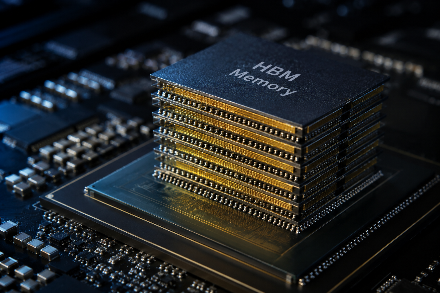
Unlike conventional memory modules, which place memory chips side by side on a circuit board, HBM stacks multiple memory chips vertically. These stacked chips are connected using microscopic vertical electrical pathways known as Through-Silicon Vias (TSVs).
The entire memory stack sits extremely close to the processor, usually on the same silicon package using a special silicon base called an interposer. This short physical distance allows data to travel much faster while reducing energy consumption.
The goal of HBM is not necessarily to achieve the highest clock speeds. Instead, it achieves exceptional performance by allowing an enormous amount of data to move simultaneously through a very wide communication pathway.
Why Modern Computers Need Faster Memory
Processors have improved dramatically over the past several decades.
Modern CPUs contain dozens of processing cores.
Graphics processors contain thousands of parallel computing units.
AI accelerators can perform trillions of mathematical operations every second.
However, these incredibly powerful processors are only as fast as the memory feeding them with data.
Imagine an expert chef preparing hundreds of meals every hour. If ingredients arrive slowly, the chef spends much of the day waiting instead of cooking.
The same thing happens inside computers.
Even the fastest processor cannot perform calculations if the required data has not yet arrived from memory.
This limitation is commonly known as the memory bottleneck.
HBM was created specifically to eliminate this bottleneck.
What Does “Bandwidth” Mean?
One of the defining features of HBM is its exceptionally high bandwidth.
Memory bandwidth refers to the amount of data that can move between memory and a processor every second.
A useful analogy is a highway.
Clock speed is similar to how fast cars can drive.
Bandwidth is similar to how many lanes the highway has.
A narrow road may allow fast cars, but traffic still becomes congested.
A much wider highway allows many more vehicles to travel simultaneously.
HBM dramatically widens the memory “highway,” allowing vast quantities of information to move at once.
For AI systems processing billions of numbers simultaneously, this enormous bandwidth is far more valuable than simply increasing memory frequency.
How HBM Is Built
HBM looks very different from traditional memory.
Instead of arranging memory chips flat across a circuit board, engineers stack multiple DRAM dies vertically.
Each layer contains memory cells that store digital information.
Tiny vertical holes are drilled through the silicon layers.
These holes are filled with conductive material, creating Through-Silicon Vias.
TSVs connect every memory layer directly to the layers above and below.
The completed stack may contain eight, twelve, or even sixteen memory dies depending on the HBM generation.
The memory stack is then mounted beside the processor on a silicon interposer.
The interposer contains thousands of microscopic electrical connections linking memory directly to the processor.
Because these connections are incredibly short, signals travel quickly while consuming less electrical power.
Through-Silicon Vias: The Secret Behind HBM
Through-Silicon Vias are one of HBM’s greatest engineering breakthroughs.
Traditional memory communicates through wires running across the surface of circuit boards.
HBM instead creates direct vertical connections through the silicon itself.
Each TSV is only a tiny fraction of a millimeter wide.
Thousands of these microscopic pathways work together simultaneously.
The result is dramatically shorter communication distances.
Shorter electrical paths reduce resistance, improve signal quality, lower latency, and reduce power consumption.
Without TSV technology, modern HBM would not be possible.
What Is a Silicon Interposer?
The silicon interposer acts as an ultra-high-speed communication platform.
It is a thin piece of silicon containing thousands of tiny electrical pathways.
The processor and HBM memory stacks are mounted directly on top of this interposer.
Instead of traveling several centimeters across a motherboard, electrical signals travel only a few millimeters.
This dramatically increases communication speed.
The interposer also supports thousands of parallel data connections that would be impossible using conventional packaging methods.
Why HBM Is So Much Faster
Many people assume HBM is faster because it runs at extremely high frequencies.
That is only part of the story.
HBM’s greatest advantage comes from its extraordinarily wide memory interface.
Conventional memory often transfers data across relatively narrow communication channels.
HBM uses interfaces thousands of bits wide.
This allows far more data to move during every clock cycle.
Instead of relying solely on speed, HBM increases the amount of information transferred simultaneously.
The result is memory bandwidth that can exceed one terabyte per second in modern HBM generations.
This makes HBM ideal for workloads involving enormous datasets.
HBM vs Traditional DDR Memory
Most desktop and laptop computers use DDR memory.
DDR memory is affordable, flexible, and available in large capacities.
However, DDR modules sit several centimeters away from the processor on the motherboard.
Data must travel relatively long electrical paths.
HBM places memory directly beside the processor.
Communication distances become dramatically shorter.
HBM also provides significantly higher bandwidth.
On the other hand, DDR memory is much less expensive and easier to upgrade.
Because HBM is integrated into the processor package, users generally cannot replace or upgrade it.
For everyday computing tasks such as web browsing, office work, and media playback, DDR memory remains the practical choice.
HBM is designed for applications where maximum performance matters more than upgradeability.
HBM vs GDDR Memory
Graphics cards have traditionally relied on GDDR memory.
GDDR is specifically optimized for graphics workloads.
Modern gaming GPUs still use GDDR6 or GDDR7 because they provide excellent performance at relatively reasonable cost.
HBM offers substantially greater bandwidth and better power efficiency.
However, it is also more expensive to manufacture.
Because gaming graphics cards must remain affordable for millions of consumers, manufacturers often choose GDDR instead of HBM.
Professional AI accelerators and data-center GPUs, where performance is the highest priority, increasingly rely on HBM.
The Evolution of HBM
HBM technology has evolved rapidly.
The first generation introduced stacked memory architecture and dramatically improved bandwidth compared with existing technologies.
HBM2 increased capacity and transfer speed while becoming widely adopted in professional computing.
HBM2E further expanded bandwidth and memory density, supporting increasingly demanding AI and high-performance computing workloads.
HBM3 represented another major leap, delivering much higher bandwidth and larger capacities.
HBM3E improved upon HBM3 with even greater transfer rates and efficiency, making it especially valuable for today’s generative AI systems.
Engineers are already developing future generations that promise even higher capacities and faster communication.
Each new generation helps satisfy the rapidly growing computational demands of artificial intelligence.
Why Artificial Intelligence Depends on HBM
Artificial intelligence processes astonishing amounts of information.
Large language models may contain hundreds of billions of parameters.
Training these models requires processors to continuously read and write enormous volumes of data.
If memory cannot keep up, expensive AI accelerators spend valuable time idle.
HBM solves this challenge by delivering data fast enough to keep AI processors fully utilized.
This is one reason why nearly every cutting-edge AI accelerator now incorporates HBM.
As AI models continue growing larger, memory bandwidth becomes just as important as processing power.
HBM in AI Accelerators
Today’s AI chips perform trillions of calculations every second.
These processors require constant access to weights, activations, training data, and intermediate results.
HBM allows these enormous datasets to remain close to the processor.
This reduces delays and improves overall computational efficiency.
Without HBM, many modern AI workloads would run significantly slower.
As AI becomes increasingly central to scientific research, healthcare, robotics, and cloud computing, HBM continues growing in importance.
HBM in Graphics Processing Units
Professional GPUs perform much more than graphics rendering.
They accelerate machine learning, scientific simulations, engineering analysis, video production, and financial modeling.
These workloads involve processing massive datasets simultaneously.
HBM provides the bandwidth required to feed thousands of GPU cores without creating memory bottlenecks.
Some of the world’s fastest graphics processors therefore rely on HBM rather than conventional graphics memory.
HBM in Supercomputers
Supercomputers solve some of humanity’s most complex scientific challenges.
They simulate climate systems.
Model earthquakes.
Study galaxies.
Design new medicines.
Analyze DNA.
Predict weather.
Perform nuclear research.
These enormous calculations require processors to exchange incredible amounts of information.
HBM enables this continuous flow of data, allowing supercomputers to reach extraordinary performance levels.
Many of the world’s fastest supercomputers incorporate HBM-based processors.
HBM in Data Centers
Modern cloud services increasingly rely on AI.
Every recommendation system, image generator, chatbot, search engine, and language model requires enormous computational resources.
Cloud providers deploy thousands of AI accelerators working together.
HBM helps these accelerators operate efficiently while reducing energy consumption.
Since electricity represents a major operating cost for large data centers, HBM’s improved efficiency provides significant economic advantages.
Why HBM Uses Less Power
One surprising advantage of HBM is its energy efficiency.
Although HBM delivers much higher bandwidth than conventional memory, it often consumes less energy for each bit transferred.
Several factors contribute to this efficiency.
The memory sits physically closer to the processor.
Electrical signals travel much shorter distances.
Operating voltages can be lower.
Wide communication channels reduce the need for extremely high clock speeds.
Lower energy consumption reduces heat generation.
This helps maintain system reliability while lowering cooling requirements.
Challenges of HBM
Despite its impressive capabilities, HBM is not without limitations.
Manufacturing HBM is extremely complex.
Stacking multiple silicon dies requires extraordinary precision.
Producing reliable Through-Silicon Vias is technically demanding.
Silicon interposers are also expensive to manufacture.
Assembling processors with HBM involves advanced semiconductor packaging technologies unavailable at many fabrication facilities.
These manufacturing challenges contribute to HBM’s high cost.
Limited production capacity has also made HBM one of the most sought-after semiconductor technologies during the AI boom.
Why HBM Is More Expensive
HBM costs considerably more than conventional memory.
Several reasons explain this.
The manufacturing process is much more sophisticated.
Memory chips must be stacked precisely.
Thousands of TSV connections must function perfectly.
Advanced packaging technologies increase production costs.
Testing stacked memory systems is also more challenging than testing individual memory chips.
Because demand for AI hardware has surged rapidly, manufacturers have struggled to expand production fast enough.
This combination of technological complexity and enormous demand has made HBM one of the most valuable products in the semiconductor industry.
The Companies Making HBM
Only a handful of companies possess the expertise required to manufacture advanced HBM.
Major memory manufacturers invest billions of dollars in developing new HBM technologies.
These companies continuously improve memory density, bandwidth, power efficiency, and manufacturing techniques.
As AI infrastructure expands worldwide, competition in HBM development has become one of the semiconductor industry’s most strategically important areas.
The Future of HBM
HBM continues evolving rapidly.
Future generations are expected to provide even greater bandwidth, larger capacities, and improved energy efficiency.
Researchers are exploring taller memory stacks, faster interfaces, advanced packaging technologies, and new materials that could further increase performance.
Future processors may integrate even larger amounts of HBM directly into computing packages.
As artificial intelligence models become increasingly sophisticated, demand for high-bandwidth memory is likely to continue rising.
HBM may also become more common beyond supercomputers and AI servers as manufacturing techniques mature and production costs decline.
Why HBM Matters More Than Ever
The modern computing revolution is no longer driven solely by faster processors. Memory has become just as important. Powerful AI chips, advanced graphics processors, and scientific supercomputers all require an uninterrupted stream of data to reach their full potential.
HBM represents one of the most significant advances in memory technology because it addresses this challenge directly. By stacking memory vertically, connecting layers through microscopic Through-Silicon Vias, and placing memory next to processors using advanced packaging, HBM delivers extraordinary bandwidth while improving energy efficiency.
As artificial intelligence, cloud computing, scientific research, and high-performance computing continue to expand, HBM will remain one of the essential technologies enabling future breakthroughs. Although most people may never see an HBM chip inside their devices, its impact will increasingly shape the speed, intelligence, and capabilities of the digital world around us.